LTC2234IUK Linear Technology, LTC2234IUK Datasheet - Page 5
LTC2234IUK
Manufacturer Part Number
LTC2234IUK
Description
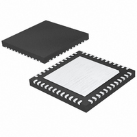
IC ADC 10BIT 135MSPS SAMPL 48QFN
Manufacturer
Linear Technology
Datasheet
1.LTC2234IUKPBF.pdf
(24 pages)
Specifications of LTC2234IUK
Number Of Bits
10
Sampling Rate (per Second)
135M
Data Interface
Parallel
Number Of Converters
1
Power Dissipation (max)
680mW
Voltage Supply Source
Single Supply
Operating Temperature
-40°C ~ 85°C
Mounting Type
Surface Mount
Package / Case
48-WFQFN, Exposed Pad
Lead Free Status / RoHS Status
Contains lead / RoHS non-compliant
Available stocks
Company
Part Number
Manufacturer
Quantity
Price
Company:

Part Number:
LTC2234IUK#PBF
Manufacturer:
Linear Technology
Quantity:
135


range, otherwise specifications are at T
range, otherwise specifications are at T
SYMBOL
V
OV
I
P
P
P
SYMBOL
f
t
t
t
t
t
t
Pipeline Latency
Note 1: Stresses beyond those listed under Absolute Maximum Ratings
may cause permanent damage to the device. Exposure to any Absolute
Maximum Rating condition for extended periods may affect device
reliability and lifetime.
Note 2: All voltage values are with respect to ground with GND and OGND
wired together (unless otherwise noted).
Note 3: When these pin voltages are taken below GND or above V
be clamped by internal diodes. This product can handle input currents of
greater than 100mA below GND or above V
Note 4: V
ENC
unless otherwise noted.
POWER REQUIRE E TS
TI I G CHARACTERISTICS
VDD
S
L
H
AP
OE
D
C
DD
DISS
SHDN
NAP
DD
W
+
/ENC
U
–
DD
= 2V
= 3.3V, OV
P-P
PARAMETER
Analog Supply Voltage
Output Supply Voltage
Analog Supply Current
Power Dissipation
Shutdown Power
Nap Mode Power
PARAMETER
Sampling Frequency
ENC Low Time
ENC High Time
Sample-and-Hold Aperture Delay
Output Enable Delay
ENC to DATA Delay
ENC to CLOCKOUT Delay
DATA to CLOCKOUT Skew
sine wave, input range = 2V
DD
= 1.8V, f
W U
SAMPLE
DD
A
A
(Note 7)
SHDN = High, OE = Low, No CLK
without latchup.
CONDITIONS
(Note 7)
SHDN = High, OE = High, No CLK
= 25°C. (Note 4)
= 25°C. (Note 8)
P-P
= 135MHz, differential
with differential drive,
CONDITIONS
Duty Cycle Stabilizer Off
Duty Cycle Stabilizer On
Duty Cycle Stabilizer Off
Duty Cycle Stabilizer On
(Note 7)
(Note 7)
(Note 7)
(t
C
The
- t
D
The
) (Note 7)
●
DD
denotes the specifications which apply over the full operating temperature
●
, they will
denotes the specifications which apply over the full operating temperature
Note 5: Integral nonlinearity is defined as the deviation of a code from a
straight line passing through the actual endpoints of the transfer curve. The
deviation is measured from the center of the quantization band.
Note 6: Offset error is the offset voltage measured from –0.5 LSB when the
output code flickers between 00 0000 0000 and 11 1111 1111 in 2’s
complement output mode.
Note 7: Guaranteed by design, not subject to test.
Note 8: V
ENC
output C
+
/ENC
LOAD
–
DD
= 2V
= 5pF.
= 3.3V, OV
P-P
sine wave, input range = 1V
DD
●
●
●
●
●
●
●
●
●
●
●
●
●
= 1.8V, f
MIN
MIN
–0.6
3.1
0.5
3.5
3.5
1.3
1.3
1
2
2
SAMPLE
TYP
TYP
191
630
3.3
3.3
3.7
3.7
3.7
3.7
2.1
2.1
35
2
0
5
0
5
P-P
= 135MHz, differential
LTC2234
with differential drive,
MAX
MAX
206
680
135
500
500
500
500
3.5
3.6
3.5
3.5
0.6
10
UNITS
UNITS
Cycles
2234fa
5
MHz
mW
mW
mW
mA
ns
ns
ns
ns
ns
ns
ns
ns
ns
V
V
Related parts for LTC2234IUK
Image
Part Number
Description
Manufacturer
Datasheet
Request
R

Part Number:
Description:
10-Bit 135Msps ADC
Manufacturer:
Linear Technology
Datasheet:
Part Number:
Description:
CD ROM LINEARVIEW DATASHEETS
Manufacturer:
Linear Technology

Part Number:
Description:
Standalone Linear Li-Ion Battery Charger with Thermal Regulation in ThinSOT
Manufacturer:
Linear Technology Corporation
Datasheet:
Part Number:
Description:
Low noise, high frequency, 8th order linear phase lowpass filter
Manufacturer:
Linear Technology Corporation
Datasheet:
Part Number:
Description:
Manufacturer:
Linear Technology Corporation
Datasheet:
Part Number:
Description:
Manufacturer:
Linear Technology Corporation
Datasheet:
Part Number:
Description:
Manufacturer:
Linear Technology Corporation
Datasheet:
Part Number:
Description:
Manufacturer:
Linear Technology Corporation
Datasheet:
Part Number:
Description:
Manufacturer:
Linear Technology Corporation
Datasheet:
Part Number:
Description:
Manufacturer:
Linear Technology Corporation
Datasheet:
Part Number:
Description:
Manufacturer:
Linear Technology Corporation
Datasheet:
Part Number:
Description:
Dual and Quad, JFET Input Precision High Speed Op Amps
Manufacturer:
Linear Technology Corporation
Datasheet:
Part Number:
Description:
Manufacturer:
Linear Technology Corporation
Datasheet:
Part Number:
Description:
1, 2, 6 and 8 Channel, 10-Bit Serial I/O Data Acquisition Systems
Manufacturer:
Linear Technology Corporation
Datasheet:
Part Number:
Description:
Manufacturer:
Linear Technology Corporation
Datasheet: