HI7188IN Intersil, HI7188IN Datasheet - Page 10
HI7188IN
Manufacturer Part Number
HI7188IN
Description
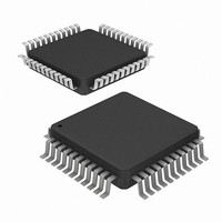
CONV A/D 16BIT 8:1 MUX 44-MQFP
Manufacturer
Intersil
Datasheet
1.HI7188IN.pdf
(24 pages)
Specifications of HI7188IN
Number Of Bits
16
Sampling Rate (per Second)
240
Data Interface
QSPI™, Serial, SPI™
Number Of Converters
1
Power Dissipation (max)
50mW
Voltage Supply Source
Analog and Digital, Dual ±
Operating Temperature
-40°C ~ 85°C
Mounting Type
Surface Mount
Package / Case
44-QFP
Lead Free Status / RoHS Status
Contains lead / RoHS non-compliant
Available stocks
Company
Part Number
Manufacturer
Quantity
Price


Functional Description
The HI7188 contains a differential 8 channel multiplexer,
Programmable Gain Instrumentation Amplifier (PGIA), 4th
order sigma-delta ADC, integrating filter, line noise rejection
filters, Calibration and data RAMs, bidirectional serial port,
clock oscillator, and a microsequencer. The 8 to 1
multiplexer at the input combined with the resetable
modulator on the HI7188 allow for conversions of up to 8
differential channels with each channel being updated at a
rate of 240 samples per second (with 60Hz line noise
rejection enabled). The device can be programmed for
conversion of any combination of physical channels. After
the signal has passed through the multiplexer, it moves into
the PGIA. The PGIA can be configured in gains of 1, 2, 4
and 8 specific for each of the 8 logical channels. The signal
then enters the sigma delta modulator. The patented one-
shot sigma delta modulator is a fourth order modulator which
converts the differential analog signal into a series of one bit
outputs. The 1’s density of this data stream provides a digital
representation of the analog input. The output of the
modulator is fed into the integrating low pass digital filter.
Data out of the filter is available after 201 bits are received
from the modulator.
If the device is in line noise rejection mode, the integrating
filter data is routed to the Line Noise Rejection filters. This
data is then calibrated using the offset and gain calibration
coefficients. Data coding is performed and the result is
stored in the data RAM. If line noise rejection is disabled, the
averaging filter is bypassed, calibration is performed on the
data from the integrating filter, the data is coded, and the
result is stored in the data RAM.
This data flow of modulation, filter and calibrate is repeated
for each of the active logical channels (up to 8). After all
active logical channels are converted the HI7188 generates
an active low interrupt, End Of Scan (EOS), that indicates all
logical channels have been updated and valid data is
available to be read from the data RAM.
Converted data is read via the HI7188 serial I/O port which
is compatible with most synchronous transfer formats
including both the Motorola SPI and Intel 8051 series SSR
protocols. All RAMs, including the Data RAM, are accessed
in a “burst” mode. That is, the data for all active logical
channels is accessed in a single read communication cycle.
Using the HI7188
This section describes how to use the device for a typical
application. This includes power supply considerations, initial
reset, calibration and conversion. Please refer to Figure 7.
The analog and digital supplies and grounds are separate
on the HI7188 to minimize digital noise coupling into the
analog circuitry. Nominal supply voltages are AV
DV
for AV
DD
DD
= +5V, and AV
and DV
DD
it is imperative that the supply is
SS
= -5V. If the same supply is used
10
DD
= +5V,
HI7188
separately decoupled to the AV
HI7188. Separate analog and digital ground planes should
be maintained on the system board and the grounds should
be tied together back at the power supply.
When the HI7188 is powered up it needs to be reset by pulling
the RST line low. This resets the internal registers as shown in
Table 1. This initial configuration defines the part for one
active logical channel (physical channel 1, address 000),
conversion mode, unipolar operation, gain of one, no line
noise rejection, offset binary coding, MSB first I/O bit order,
descending I/O byte order, and single line interface. After the
RST line returns high, the device immediately begins
converting as described above without any further instruction.
There is no correction for offset or gain errors on the
converted data at this time. To ensure maximum performance,
calibration should be done as defined in the operation mode
section.
The reset configuration should be updated to reflect the
users system including chip level and channel level
programming.
A calibration routine should be performed next to remove
system offset and full scale errors (see Calibration section).
The CCR is used to place each channel of the device in
several operational modes including Conversion, System
Offset Calibration, System Positive Full Scale Calibration
and System Negative Full Scale Calibration. Each channel
inputs should be connected and settled to the correct input
condition before the CCR is programmed for each calibration
point. After a complete system calibration is performed, the
desired analog input is applied and accurate data can be
read via the serial interface. The device should be recalibrated
when there is a change in the user configuration (i.e. gain,
unipolar/bipolar), supply voltage or ambient temperature.
Data Output Registers
Channel Configuration Register #2
Channel Configuration Register #1
Control Register
Offset Calibration Registers
Positive Full Scale Calibration Registers
Negative Full Scale Calibration Registers
1. Chip level refers to programming common to all channels
2. Channel level programming is custom for each channel
such as 50/60 Hertz Line Noise Rejection, number of
active channels, etc. and is detailed in the Control
Register (CR) section.
such as gain, physical input and mode as detailed in the
Channel Configuration Registers (CCR) section.
TABLE 1. REGISTER RESET VALUES
REGISTER
DD
and DV
XXXX (undefined)
00XXXXXX
XXXXXXXX
0000
000000
800000
800000
DD
VALUE (HEX)
pins on the
Related parts for HI7188IN
Image
Part Number
Description
Manufacturer
Datasheet
Request
R

Part Number:
Description:
8-channel, 16-bit, High Precision, Sigma-delta A/d Sub-system
Manufacturer:
Intersil Corporation
Datasheet:
Part Number:
Description:
Intersil Corporation [CMOS Serial Controller Interface]
Manufacturer:
Intersil Corporation
Datasheet:
Part Number:
Description:
Manufacturer:
Intersil Corporation
Datasheet:
Part Number:
Description:
357-036-542-201 CARDEDGE 36POS DL .156 BLK LOPRO
Manufacturer:
Intersil Corporation
Datasheet:
Part Number:
Description:
1024-Word x 4-Bit LSI Static RAM
Manufacturer:
Intersil Corporation
Datasheet:
Part Number:
Description:
General Purpose NPN Transistor Arrays FN341.4
Manufacturer:
Intersil Corporation
Datasheet:
Part Number:
Description:
CMOS 16-Bit Microprocessor
Manufacturer:
Intersil Corporation
Datasheet:
Part Number:
Description:
Manufacturer:
Intersil Corporation
Datasheet:
Part Number:
Description:
Manufacturer:
Intersil Corporation
Datasheet:
Part Number:
Description:
Manufacturer:
Intersil Corporation
Datasheet:
Part Number:
Description:
Manufacturer:
Intersil Corporation
Datasheet:
Part Number:
Description:
CMOS 6-Bit Latch and Decoder Memory Interfaces
Manufacturer:
Intersil Corporation
Datasheet:
Part Number:
Description:
CA3046General Purpose NPN Transistor Arrays
Manufacturer:
Intersil Corporation
Datasheet:
Part Number:
Description:
Manufacturer:
Intersil Corporation
Datasheet:
Part Number:
Description:
TR909 DLC/FLC SLIC with Low Power Standby
Manufacturer:
Intersil Corporation
Datasheet: