HI7188IN Intersil, HI7188IN Datasheet - Page 19
HI7188IN
Manufacturer Part Number
HI7188IN
Description
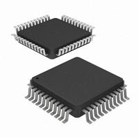
CONV A/D 16BIT 8:1 MUX 44-MQFP
Manufacturer
Intersil
Datasheet
1.HI7188IN.pdf
(24 pages)
Specifications of HI7188IN
Number Of Bits
16
Sampling Rate (per Second)
240
Data Interface
QSPI™, Serial, SPI™
Number Of Converters
1
Power Dissipation (max)
50mW
Voltage Supply Source
Analog and Digital, Dual ±
Operating Temperature
-40°C ~ 85°C
Mounting Type
Surface Mount
Package / Case
44-QFP
Lead Free Status / RoHS Status
Contains lead / RoHS non-compliant
Available stocks
Company
Part Number
Manufacturer
Quantity
Price


Detailed Register Descriptions
Instruction Register
The instruction register is an 8 bit register which is used
during a communications cycle for setting up read/write
operations. Below are the bit assignments.
R/W - Bit 7 of the Instruction Byte determines whether phase
2 of the communication cycle will be a read or write
operation. If R/W is logic 1, a write transfer will occur in
phase 2 of the communication cycle. If R/W is logic 0, a read
transfer will occur in phase 2 of the communication cycle.
NB1, NB0 - Bits 6 and 5 of the Instruction Byte determine the
number of bytes that will be transferred during phase 2 of a
communication cycle, if a register is selected for I/O access. If a
RAM is selected for IO access, these bits are don’t care. Any
number of bytes from 1 to 4 is allowed. See Tables 6 and 7.
RB - Bit 4 is used to determine the byte order when accessing
a RAM address. When accessing a RAM address, if RB = 1,
the data format is most significant byte first to least significant
byte. When accessing a RAM address, if RB = 0, the data
format is least significant byte first to most significant byte.
When accessing a register address, this bit is a don’t care.
A3, A2, A1, A0 - Bits 3 and 2 (A3 and A2) of the Instruction
Byte determine which of the three internal registers will be
accessed or if both bits are set (11b), that a RAM access is
active. For register addresses, bits 1 and 0 (A1 and A0)
determine which byte of that register will be accessed first.
For RAM access (A3 = 1, A2 = 1), bits 1 and 0 (A1 and A0)
determine which RAM is the source or destination.
IR [7]
R/W
MSB
R/W
0/1
0/1
0/1
0/1
0/1
0/1
NB1, NB0 IR [6:5]
IR [6:5]
NB1,
NB1
NB0
TABLE 7. INTERNAL REGISTER ADDRESS
00
01
00
01
00
00
TABLE 6. MULTIPLE BYTE ACCESS BITS
6
00
01
10
11
INSTRUCTION REGISTER (BYTE)
NB0
A3, A2,
IR [3:0]
A1, A0
5
0000
0000
0001
0001
0100
0101
RB
4
CR, start byte 0, 1 byte transfer
CR, start byte 0, 2 byte transfer
CR, start byte 1, 1 byte transfer
CR, start byte 1, 2 byte transfer
CCR #1, start byte 0, 1 byte transfer
CCR #1, start byte 1, 1 byte transfer
19
A3
3
Transfer 2 Bytes
Transfer 3 Bytes
Transfer 4 Bytes
DESCRIPTION
Transfer 1 Byte
DESCRIPTION
A2
2
A1
1
LSB
A0
HI7188
IR [7]
R/W
0/1
0/1
0/1
0/1
0/1
0/1
0/1
0/1
0/1
0/1
0/1
0/1
0/1
0/1
0/1
0/1
0/1
0/1
0/1
0/1
0/1
0/1
0/1
0/1
0/1
0/1
0/1
0/1
0/1
0/1
0/1
0/1
0/1
0/1
0/1
0/1
0
0
TABLE 7. INTERNAL REGISTER ADDRESS (Continued)
IR [6:5]
NB1,
NB0
00
00
01
01
01
01
10
10
10
10
11
11
11
11
00
00
00
00
01
01
01
01
10
10
10
10
11
11
11
11
xx
xx
xx
xx
xx
xx
xx
xx
A3, A2,
IR [3:0]
A1, A0
0110
0111
0100
0101
0110
0111
0100
0101
0110
0111
0100
0101
0110
0111
1000
1001
1010
1011
1000
1001
1010
1011
1000
1001
1010
1011
1000
1001
1010
1011
1100
1100
1101
1101
1110
1110
1111
1111
CCR #1, start byte 2, 1 byte transfer
CCR #1, start byte 3, 1 byte transfer
CCR #1, start byte 0, 2 byte transfer
CCR #1, start byte 1, 2 byte transfer
CCR #1, start byte 2, 2 byte transfer
CCR #1, start byte 3, 2 byte transfer
CCR #1, start byte 0, 3 byte transfer
CCR #1, start byte 1, 3 byte transfer
CCR #1, start byte 2, 3 byte transfer
CCR #1, start byte 3, 3 byte transfer
CCR #1, start byte 0, 4 byte transfer
CCR #1, start byte 1, 4 byte transfer
CCR #1, start byte 2, 4 byte transfer
CCR #1, start byte 3, 4 byte transfer
CCR #2, start byte 0, 1 byte transfer
CCR #2, start byte 1, 1 byte transfer
CCR #2, start byte 2, 1 byte transfer
CCR #2, start byte 3, 1 byte transfer
CCR #2, start byte 0, 2 byte transfer
CCR #2, start byte 1, 2 byte transfer
CCR #2, start byte 2, 2 byte transfer
CCR #2, start byte 3, 2 byte transfer
CCR #2, start byte 0, 3 byte transfer
CCR #2, start byte 1, 3 byte transfer
CCR #2, start byte 2, 3 byte transfer
CCR #2, start byte 3, 3 byte transfer
CCR #2, start byte 0, 4 byte transfer
CCR #2, start byte 1, 4 byte transfer
CCR #2, start byte 2, 4 byte transfer
CCR #2, start byte 3, 4 byte transfer
Data
significant byte first, READ ONLY
Data
significant byte first, READ ONLY
Offset RAM burst transfer, least
significant byte first.
Offset RAM burst transfer, most
significant byte first.
Positive full scale RAM burst transfer,
least significant byte first.
Positive full scale RAM burst transfer,
most significant byte first.
Negative full scale RAM burst transfer,
least significant byte first.
Negative full scale RAM burst transfer,
most significant byte first.
RAM
RAM
DESCRIPTION
burst
burst
transfer,
transfer,
most
least
Related parts for HI7188IN
Image
Part Number
Description
Manufacturer
Datasheet
Request
R

Part Number:
Description:
8-channel, 16-bit, High Precision, Sigma-delta A/d Sub-system
Manufacturer:
Intersil Corporation
Datasheet:
Part Number:
Description:
Intersil Corporation [CMOS Serial Controller Interface]
Manufacturer:
Intersil Corporation
Datasheet:
Part Number:
Description:
Manufacturer:
Intersil Corporation
Datasheet:
Part Number:
Description:
357-036-542-201 CARDEDGE 36POS DL .156 BLK LOPRO
Manufacturer:
Intersil Corporation
Datasheet:
Part Number:
Description:
1024-Word x 4-Bit LSI Static RAM
Manufacturer:
Intersil Corporation
Datasheet:
Part Number:
Description:
General Purpose NPN Transistor Arrays FN341.4
Manufacturer:
Intersil Corporation
Datasheet:
Part Number:
Description:
CMOS 16-Bit Microprocessor
Manufacturer:
Intersil Corporation
Datasheet:
Part Number:
Description:
Manufacturer:
Intersil Corporation
Datasheet:
Part Number:
Description:
Manufacturer:
Intersil Corporation
Datasheet:
Part Number:
Description:
Manufacturer:
Intersil Corporation
Datasheet:
Part Number:
Description:
Manufacturer:
Intersil Corporation
Datasheet:
Part Number:
Description:
CMOS 6-Bit Latch and Decoder Memory Interfaces
Manufacturer:
Intersil Corporation
Datasheet:
Part Number:
Description:
CA3046General Purpose NPN Transistor Arrays
Manufacturer:
Intersil Corporation
Datasheet:
Part Number:
Description:
Manufacturer:
Intersil Corporation
Datasheet:
Part Number:
Description:
TR909 DLC/FLC SLIC with Low Power Standby
Manufacturer:
Intersil Corporation
Datasheet: