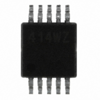
ISL22414WFU10Z Intersil, ISL22414WFU10Z Datasheet - Page 12

ISL22414WFU10Z
Manufacturer Part Number
ISL22414WFU10Z
Description
IC POT DGTL 256TP LN LP 10-MSOP
Manufacturer
Intersil
Series
XDCP™r
Datasheet
1.ISL22414WFU10Z.pdf
(16 pages)
Specifications of ISL22414WFU10Z
Taps
256
Resistance (ohms)
10K
Number Of Circuits
1
Temperature Coefficient
±50ppm/°C
Memory Type
Non-Volatile
Interface
SPI Serial
Voltage - Supply
±2.25 V ~ 5.5 V
Operating Temperature
-40°C ~ 125°C
Mounting Type
Surface Mount
Package / Case
10-MSOP, Micro10™, 10-uMAX, 10-uSOP
Resistance In Ohms
10K
Lead Free Status / RoHS Status
Lead free / RoHS Compliant
Available stocks
Company
Part Number
Manufacturer
Quantity
Price
Company:
Part Number:
ISL22414WFU10Z
Manufacturer:
Intersil
Quantity:
500
Company:
Part Number:
ISL22414WFU10Z-T7A
Manufacturer:
INTERSIL
Quantity:
1 001
All communication over the SPI interface is conducted by
sending the MSB of each byte of data first.
Protocol Conventions
The SPI protocol contains Instruction Byte followed by one
or more Data Bytes. A valid Instruction Byte contains
instruction as the three MSBs, with the following five register
address bits (see Table 3).
The next byte sent to the ISL22414 is the Data Byte.
Table 4 contains a valid instruction set for ISL22414.
There are only sixteen register addresses possible for this
DCP. If the [R4:R0] bits are zero, then the read or write is to
either the IVR or the WR register (depends of VOL bit at
ACR). If the [R4:R0] are 10000, then the operation is on the
ACR.
Write Operation
A Write operation to the ISL22414 is a two or more bytes
operation. It requires first, the CS transition from HIGH to
where X means “do not care”
BIT #
I2
0
0
0
1
1
I2
7
SDO
SCK
TABLE 3. INSTRUCTION BYTE FORMAT
SDI
CS
I1
0
0
1
0
1
I1
6
I0
5
I0
0
1
1
0
0
WR INSTRUCTION
12
R4
4
INSTRUCTION SET
1
R4
R4
R4
X
X
X
R3
3
2
R2
2
3
FIGURE 16. TWO BYTE WRITE SEQUENCE
R3
R3
R3
X
X
X
4
R1
1
TABLE 4. INSTRUCTION SET
R2
5
R2
R2
X
X
X
R0
ADDR
0
ISL22414
6
R1
R1
R1
X
X
X
7
LOW. Then host send a valid Instruction Byte, followed by
one or more Data Bytes to SDI pin. The host terminates the
write operation by pulling the CS pin from LOW to HIGH.
Instruction is executed on rising edge of CS. For a write to
address 0, the MSB of the byte at address 10h (ACR[7])
determines if the Data Byte is to be written to volatile or both
volatile and non-volatile registers. Refer to “Memory
Description” and Figure 16. Note, the internal non-volatile
write cycle starts with the rising edge of CS and requires up
to 20ms. During non-volatile write cycle the read operation to
ACR register is allowed to check WIP bit.
Read Operation
A Read operation to the ISL22414 is a four byte operation. It
requires first, the CS transition from HIGH to LOW. Then
host send a valid Instruction Byte, followed by “dummy” Data
Byte, NOP Instruction Byte and another “dummy” Data Byte
to SDI pin. The SPI host receives the Instruction Byte
(instruction code + register address) and requested Data
Byte from SDO pin on the rising edge of SCK during third
and fourth bytes respectively. The host terminates the read
operation by pulling the CS pin from LOW to HIGH (see
Figure 17). Reading from the IVR will not change the WR, if
its contents are different.
8
R0
R0
R0
X
X
X
9
NOP
ACR READ
ACR WRITE
WR, IVR, GP or ACR READ
WR, IVR, GP or ACR WRITE
10
11
DATA BYTE
12
OPERATION
13
14
15
December 16, 2010
16
FN6424.1


