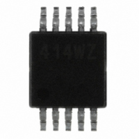
ISL22414WFU10Z Intersil, ISL22414WFU10Z Datasheet - Page 13

ISL22414WFU10Z
Manufacturer Part Number
ISL22414WFU10Z
Description
IC POT DGTL 256TP LN LP 10-MSOP
Manufacturer
Intersil
Series
XDCP™r
Datasheet
1.ISL22414WFU10Z.pdf
(16 pages)
Specifications of ISL22414WFU10Z
Taps
256
Resistance (ohms)
10K
Number Of Circuits
1
Temperature Coefficient
±50ppm/°C
Memory Type
Non-Volatile
Interface
SPI Serial
Voltage - Supply
±2.25 V ~ 5.5 V
Operating Temperature
-40°C ~ 125°C
Mounting Type
Surface Mount
Package / Case
10-MSOP, Micro10™, 10-uMAX, 10-uSOP
Resistance In Ohms
10K
Lead Free Status / RoHS Status
Lead free / RoHS Compliant
Available stocks
Company
Part Number
Manufacturer
Quantity
Price
Company:
Part Number:
ISL22414WFU10Z
Manufacturer:
Intersil
Quantity:
500
Company:
Part Number:
ISL22414WFU10Z-T7A
Manufacturer:
INTERSIL
Quantity:
1 001
Applications Information
Communicating with ISL22414
Communication with ISL22414 proceeds using SPI interface
through the ACR (address 10000b), IVR (address 00000b),
WR (addresses 00000b) and General Purpose registers
(addresses from 00001b to 01110b).
The wiper of the potentiometer is controlled by the WR
register. Writes and reads can be made directly to these
register to control and monitor the wiper position without any
non-volatile memory changes. This is done by setting MSB
bit at address 10000b to 1 (ACR[7] = 1).
The non-volatile IVR stores the power up position of the
wiper. IVR is accessible when MSB bit at address 10000b is
set to 0 (ACR[7] = 0). Writing a new value to the IVR register
will set a new power up position for the wiper. Also, writing to
this register will load the same value into the corresponding
WR as the IVR. Reading from the IVR will not change the
WR, if its contents are different.
Daisy Chain Configuration
When application needs more then one ISL22414, it can
communicate with all of them without additional CS lines by
daisy chaining the DCPs as shown on Figure 18. In Daisy
Chain configuration the SDO pin of previous chip is
connected to SDI pin of the following chip, and each CS and
SCK pins are connected to the corresponding
microcontroller pins in parallel, like regular SPI interface
implementation. The Daisy Chain configuration can also be
used for simultaneous setting of multiple DCPs. Note, the
number of daisy chained DCPs is limited only by the driving
capabilities of SCK and CS pins of microcontroller; for larger
number of SPI devices buffering of SCK and CS lines is
required.
Daisy Chain Write Operation
The write operation starts by HIGH to LOW transition on CS
line, followed by N number of two bytes write instructions on
SDI line with reversed chain access sequence: the
instruction byte + data byte for the last DCP in chain is going
first, as shown on Figure 19, where N is a number of DCPs
in chain. The serial data is going through DCPs from DCP0
SCK
SDO
SDI
CS
1
RD
13
ADDR
FIGURE 17. FOUR BYTE READ SEQUENCE
8
ISL22414
to DCP(N-1) as follow: DCP0 --> DCP1 --> DCP2 --> ... -->
DCP(N-1). The write instruction is executed on the rising
edge of CS for all N DCPs simultaneously.
Daisy Chain Read Operation
The read operation consists two parts: first, send read
instructions (N two bytes operation) with valid address;
second, read the requested data while sending NOP
instructions (N two bytes operation) as shown on Figure 20,
and Figure 21.
The first part starts by HIGH to LOW transition on CS line,
followed by N two bytes read instruction on SDI line with
reversed chain access sequence: the instruction byte +
dummy data byte for the last DCP in chain is going first,
followed by LOW to HIGH transition on CS line. The read
instructions are executed during second part of read
sequence. It also starts by HIGH to LOW transition on CS
line, followed by N number of two bytes NOP instructions on
SDI line and LOW to HIGH transition of CS. The data is read
on every even byte during second part of read sequence
while every odd byte contains instruction code + address
from which the data is being read.
Wiper Transition
When stepping up through each tap in voltage divider mode,
some tap transition points can result in noticeable voltage
transients, or overshoot/undershoot, resulting from the
sudden transition from a very low impedance “make” to a
much higher impedance “break within an extremely short
period of time (<50ns). Two such code transitions are EFh to
F0h, and 0Fh to 10h. Note, that all switching transients will
settle well within the settling time as stated in the datasheet.
A small capacitor can be added externally to reduce the
amplitude of these voltage transients, but that will also
reduce the useful bandwidth of the circuit, thus may not be a
good solution for some applications. It may be a good idea,
in that case, to use fast amplifiers in a signal chain for fast
recovery.
16
NOP
RD
ADDR
24
READ DATA
December 16, 2010
32
FN6424.1


