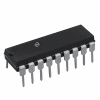
DAC1218LCJ National Semiconductor, DAC1218LCJ Datasheet - Page 2

DAC1218LCJ
Manufacturer Part Number
DAC1218LCJ
Description
IC DAC 12BIT 18-DIP
Manufacturer
National Semiconductor
Datasheet
1.DAC1218LCJ.pdf
(12 pages)
Specifications of DAC1218LCJ
Settling Time
1µs
Number Of Bits
12
Number Of Converters
1
Voltage Supply Source
Single Supply
Power Dissipation (max)
500mW
Operating Temperature
-40°C ~ 85°C
Mounting Type
Through Hole
Package / Case
*
Case
DIP-18L
Lead Free Status / RoHS Status
Contains lead / RoHS non-compliant
Data Interface
-
Other names
*DAC1218LCJ
Available stocks
Company
Part Number
Manufacturer
Quantity
Price
Company:
Part Number:
DAC1218LCJ
Manufacturer:
SIPEX
Quantity:
281
Part Number:
DAC1218LCJ
Manufacturer:
NS/国半
Quantity:
20 000
Company:
Part Number:
DAC1218LCJ-1
Manufacturer:
ON
Quantity:
19
Company:
Part Number:
DAC1218LCJ-1
Manufacturer:
MOT
Quantity:
2
Resolution
Linearity Error
(End Point Linearity)
Differential Non-Linearity
Monotonicity
Gain Error (Min)
Gain Error (Max)
Gain Error Tempco
Power Supply Rejection
Reference Input Resistance
Output Feedthrough Error
Output Capacitance
Supply Current Drain
Output Leakage Current
Digital Input Threshold
Digital Input Currents
t
s
Absolute Maximum Ratings
If Military Aerospace specified devices are required
please contact the National Semiconductor Sales
Office Distributors for availability and specifications
Supply Voltage (V
Voltage at Any Digital Input
Voltage at V
Storage Temperature Range
Package Dissipation at T
DC Voltage Applied to I
Lead Temp (Soldering 10 seconds)
ESD Susceptibility (Note 11)
Electrical Characteristics
V
Note 9) all other limits T
I
I
Current Settling Time
REF
OUT1
OUT2
(Note 4)
e
Parameter
10 000 V
REF
Input
CC
DC
)
V
OUT1
CC
A
A
e
e
e
25 C (Note 3)
or I
11 4 V
Zero and Full-Scale
Adjusted
DAC1218
DAC1219
Zero and Full-Scale
Adjusted
DAC1218
DAC1219
Using Internal R
V
All Digital Inputs High
(Min)
(Max)
V
All Data Inputs Low
All Data Inputs I
High
All Data Inputs I
Low
All Data Inputs Low
All Data Inputs High
Low Threshold
High Threshold
Digital Inputs
Digital Inputs
R
to 0 01% All Digital Inputs
Switched Simultaneously
T
J
REF
REF
OUT2
L
e
e
e
DC
e
100
25 C
120 Vp-p f
Conditions
g
to 15 75 V
b
10V
b
65 C to
Output Settled
k
l
100 mV to V
0 8V
2 2V
Fb
g
(Notes 1 and 2)
I
I
V
OUT1
OUT2
OUT1
OUT2
1V
CC
e
DC
100 kHz
a
500 mW
to GND
17 V
g
150 C
300 C
unless otherwise noted Boldface limits apply from T
800V
25V
DC
CC
2
Notes
4 5 9
4 5 9
7 9
4
5
5
5
5
9
9
6
9
9
9
Operating Conditions
Temperature Range
Range of V
Voltage at Any Digital Input
DAC1218LCJ DAC1219LCJ
DAC1218LCJ-1
(Note 10)
b
b
g
g
Typ
3 0
12
12
15
15
1
0 1
0 1
1 3
3 0
CC
(Note 11)
g
g
g
g
Tested
b
Limit
0 018
0 024
0 018
0 024
b
g
0 8
2 2
12
10
20
10
10
10
0 0
2 0
200
12
0 2
30
(Note 12)
g
g
g
g
Design
b
g
Limit
0 018
0 024
0 018
0 024
2 5
0 8
2 2
200
200
12
12
10
20
10
10
10
200
b
70
70
6 0
40 C
T
MIN
MIN s
0 C
5 V
s
to T
s
ppm of FSR V
T
DC
ppm of FS C
V
A s
T
% of FSR
% of FSR
% of FSR
% of FSR
% of FSR
% of FSR
T
CC
A s
to 16 V
MAX
A s
mVp-p
Units
V
V
Bits
Bits
mA
to GND
k
k
pF
pF
pF
pF
nA
nA
A
A
a
DC
DC
DC
DC
s
T
85 C
70 C
(see
MAX
DC


