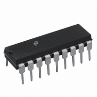
DAC1218LCJ National Semiconductor, DAC1218LCJ Datasheet - Page 4

DAC1218LCJ
Manufacturer Part Number
DAC1218LCJ
Description
IC DAC 12BIT 18-DIP
Manufacturer
National Semiconductor
Datasheet
1.DAC1218LCJ.pdf
(12 pages)
Specifications of DAC1218LCJ
Settling Time
1µs
Number Of Bits
12
Number Of Converters
1
Voltage Supply Source
Single Supply
Power Dissipation (max)
500mW
Operating Temperature
-40°C ~ 85°C
Mounting Type
Through Hole
Package / Case
*
Case
DIP-18L
Lead Free Status / RoHS Status
Contains lead / RoHS non-compliant
Data Interface
-
Other names
*DAC1218LCJ
Available stocks
Company
Part Number
Manufacturer
Quantity
Price
Company:
Part Number:
DAC1218LCJ
Manufacturer:
SIPEX
Quantity:
281
Part Number:
DAC1218LCJ
Manufacturer:
NS/国半
Quantity:
20 000
Company:
Part Number:
DAC1218LCJ-1
Manufacturer:
ON
Quantity:
19
Company:
Part Number:
DAC1218LCJ-1
Manufacturer:
MOT
Quantity:
2
Definition of Package Pinouts
(A1 –A12) Digital Inputs A12 is the least significant digital
input (LSB) and A1 is the most significant digital input
(MSB)
I
digital input of all 1s and is zero for a digital input of all 0s
I
I
voltage)
R
on the IC chip for use as the shunt feedback resistor for the
external op amp which is used to provide an output voltage
for the DAC This on-chip resistor should always be used
(not an external resistor) since it matches the resistors in
the on-chip R-2R ladder and tracks these resistors over
temperature
V
external precision voltage source to the internal R-2R lad-
der V
This is also the analog voltage input for a 4-quadrant multi-
plying DAC application
V
the part V
optimum for 15 V
GND Ground This is the ground for the circuit
Definition of Terms
Resolution Resolution is defined as the reciprocal of the
number of discrete steps in the DAC output It is directly
related to the number of switches or bits within the DAC For
example the DAC1218 has 2
has 12-bit resolution
Linearity Error Linearity error in the maximum deviation
from a straight line passing through the endpoints of the
OUT1
OUT2
OUT1
Fb
REF
CC
Feedback Resistor The feedback resistor is provided
Digital Supply Voltage This is the power supply pin for
REF
Reference Voltage Input This input connects to an
DAC Current Output 1 I
DAC Current Output 2 I
or I
can be selected over the range of 10V to
CC
OUT1
a) End point test after zero and FS adjust
can be from 5 V
a
DC
I
OUT2
e
constant (for a fixed reference
12
DC
or 4096 steps and therefore
OUT1
OUT2
to 15 V
is a maximum for a
is a constant minus
DC
Operation is
b
10V
4
DAC transfer characteristic It is measured after adjusting
for zero and full scale Linearity error is a parameter intrinsic
to the device and cannot be externally adjusted
National’s linearity test (a) and the best straight line test (b)
used by other suppliers are illustrated below The best
straight line (b) requires a special zero and FS adjustment
for each part which is almost impossible for the user to
determine The end point test uses a standard zero FS ad-
justment procedure and is a much more stringent test for
DAC linearity
Power Supply Sensitivity Power supply sensitivity is a
measure of the effect of power supply changes on the DAC
full-scale output
Settling Time Full-scale current settling time requires zero
to full-scale or full-scale to zero output change Settling time
is the time required from a code transition until the DAC
output reaches within
Full-scale Error Full-scale error is a measure of the output
error between an ideal DAC and the actual device output
Ideally for the DAC1218 full-scale is V
V
SCALE
adjustable to zero
Differential Non-Linearity The difference between any
two consecutive codes in the transfer curve from the theo-
retical 1 LSB is differential non-linearity
Monotonic If the output of a DAC increases for increasing
digital input code then the DAC is monotonic A 12-bit DAC
which is monotonic to 12 bits simply means that input in-
creasing digital input codes will produce an increasing ana-
log output
b) Shifting FS adjust to pass best straight line test
REF
e
e
10V
10 0000V
and
b
2 44 mV
g
unipolar
1 2 LSB of the final output value
e
9 9976V Full-scale error is
operation
REF
b
TL H 5691 – 3
1 LSB For
V
FULL-


