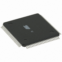
ATF1508ASV-15AU100 Atmel, ATF1508ASV-15AU100 Datasheet - Page 11

ATF1508ASV-15AU100
Manufacturer Part Number
ATF1508ASV-15AU100
Description
IC CPLD 15NS LOW V 100TQFP
Manufacturer
Atmel
Series
ATF1508ASV(L)r
Datasheet
1.ATF1508ASVL-20JU84.pdf
(28 pages)
Specifications of ATF1508ASV-15AU100
Programmable Type
In System Programmable (min 10K program/erase cycles)
Delay Time Tpd(1) Max
15.0ns
Voltage Supply - Internal
3 V ~ 3.6 V
Number Of Macrocells
128
Number Of I /o
80
Operating Temperature
-40°C ~ 85°C
Mounting Type
Surface Mount
Package / Case
100-TQFP, 100-VQFP
Voltage
3.3V
Memory Type
EEPROM
Number Of Product Terms Per Macro
40
Maximum Operating Frequency
100 MHz
Delay Time
15 ns
Number Of Programmable I/os
80
Operating Supply Voltage
3.3 V
Maximum Operating Temperature
+ 85 C
Minimum Operating Temperature
- 40 C
Mounting Style
SMD/SMT
Supply Voltage (max)
3.6 V
Supply Voltage (min)
3 V
For Use With
ATF15XX-DK3 - KIT DEV FOR ATF15XX CPLD'S
Lead Free Status / RoHS Status
Lead free / RoHS Compliant
Features
-
Number Of Logic Elements/cells
-
Lead Free Status / Rohs Status
Details
Available stocks
Company
Part Number
Manufacturer
Quantity
Price
Company:
Part Number:
ATF1508ASV-15AU100
Manufacturer:
ATMEL
Quantity:
138
Part Number:
ATF1508ASV-15AU100
Manufacturer:
ATMEL/爱特梅尔
Quantity:
20 000
Part Number:
ATF1508ASV-15AU100-T
Manufacturer:
MICROCHIP/微芯
Quantity:
20 000
Absolute Maximum Ratings*
Timing Model
1408H–PLD–7/05
Temperature Under Bias.................................. -40°C to +85°C
Storage Temperature ..................................... -65°C to +150°C
Voltage on Any Pin with
Respect to Ground .........................................-2.0V to +7.0V
Voltage on Input Pins
with Respect to Ground
During Programming.....................................-2.0V to +14.0V
Programming Voltage with
Respect to Ground .......................................-2.0V to +14.0V
Delay
Input
t
IN
Switch
Matrix
t
UIM
Register Control
Internal Output
Foldback Term
Global Control
Enable Delay
Logic Array
t
t
Delay
Delay
Delay
Delay
t
GLOB
t
t
SEXP
t
IOE
LAD
LAC
t
EN
IC
(1)
(1)
(1)
Cascade Logic
Delay
t
PEXP
Fast Input
*NOTICE:
Note:
Delay
t
FIN
1.
Stresses beyond those listed under “Absolute
Maximum Ratings” may cause permanent dam-
age to the device. This is a stress rating only and
functional operation of the device at these or any
other conditions beyond those indicated in the
operational sections of this specification is not
implied. Exposure to absolute maximum rating
conditions for extended periods may affect device
reliability.
Minimum voltage is -0.6V DC, which may under-
shoot to -2.0V for pulses of less than 20 ns. Max-
imum output pin voltage is V
which may overshoot to 7.0V for pulses of less
than 20 ns.
Register
t
Delay
COMB
t
t
t
t
PRE
CLR
t
FSU
t
SU
t
RD
FH
H
ATF1508ASV(L)
Output
Delay
t
t
t
t
t
t
OD1
OD2
OD3
t
ZX1
ZX2
ZX3
XZ
CC
+ 0.75V DC,
I/O Delay
t
IO
11


