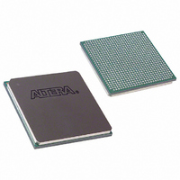
EP1S20F780I6N Altera, EP1S20F780I6N Datasheet - Page 463

EP1S20F780I6N
Manufacturer Part Number
EP1S20F780I6N
Description
IC STRATIX FPGA 20K LE 780-FBGA
Manufacturer
Altera
Series
Stratix®r
Specifications of EP1S20F780I6N
Number Of Logic Elements/cells
18460
Number Of Labs/clbs
1846
Total Ram Bits
1669248
Number Of I /o
586
Voltage - Supply
1.425 V ~ 1.575 V
Mounting Type
Surface Mount
Operating Temperature
-40°C ~ 100°C
Package / Case
780-FBGA
Family Name
Stratix
Number Of Logic Blocks/elements
18460
# I/os (max)
586
Frequency (max)
450.05MHz
Process Technology
0.13um (CMOS)
Operating Supply Voltage (typ)
1.5V
Logic Cells
18460
Ram Bits
1669248
Operating Supply Voltage (min)
1.425V
Operating Supply Voltage (max)
1.575V
Operating Temp Range
-40C to 100C
Operating Temperature Classification
Industrial
Mounting
Surface Mount
Pin Count
780
Package Type
FC-FBGA
Lead Free Status / RoHS Status
Lead free / RoHS Compliant
Number Of Gates
-
Lead Free Status / Rohs Status
Compliant
Available stocks
Company
Part Number
Manufacturer
Quantity
Price
Company:
Part Number:
EP1S20F780I6N
Manufacturer:
ALTERA
Quantity:
3 000
- Current page: 463 of 864
- Download datasheet (11Mb)
Altera Corporation
June 2006
}
As a result, the Quartus II Fitter does not count the bidirectional pin
potential outputs, and the number of V
legal range.
Toggle Rate Logic Option in Quartus II
You should specify the pin’s output toggling rate in order to perform a
stricter pad placement check in the Quartus II software. Specify the
frequency at which a pin toggles in the Quartus II Assignment Editor.
This option is useful for adjusting the pin toggle rate in order to place
them closer to differential pins. The option directs the Quartus II Fitter
toggle-rate checking while allowing you to place a single-ended pin
closer to a differential pin.
DC Guidelines
Variables affecting the DC current draw include package type and desired
termination methods. This section provides information on each of these
variables and also shows how to calculate the DC current for pin
placement.
1
For any 10 consecutive output pads in an I/O bank, Altera recommends
a maximum current of 200 mA for thermally enhanced FineLine BGA and
thermally enhanced BGA cavity up packages and 164 mA for
non-thermally enhanced cavity up and non-thermally enhanced FineLine
BGA packages. The following equation shows the current density
limitation equation for thermally enhanced FineLine BGA and thermally
enhanced BGA cavity up packages:
The following equation shows the current density limitation equation for
non-thermally enhanced cavity up and non-thermally enhanced
FineLine BGA packages:
dm : OUTPUT_ENABLE_GROUP 1;
pin + 9
Σ
pin
The Quartus II software automatically takes these variables into
account during compilation.
I
pin
< 200 mA
Selectable I/O Standards in Stratix & Stratix GX Devices
Stratix Device Handbook, Volume 2
REF
bank outputs remains in the
4–35
Related parts for EP1S20F780I6N
Image
Part Number
Description
Manufacturer
Datasheet
Request
R

Part Number:
Description:
CYCLONE II STARTER KIT EP2C20N
Manufacturer:
Altera
Datasheet:

Part Number:
Description:
CPLD, EP610 Family, ECMOS Process, 300 Gates, 16 Macro Cells, 16 Reg., 16 User I/Os, 5V Supply, 35 Speed Grade, 24DIP
Manufacturer:
Altera Corporation
Datasheet:

Part Number:
Description:
CPLD, EP610 Family, ECMOS Process, 300 Gates, 16 Macro Cells, 16 Reg., 16 User I/Os, 5V Supply, 15 Speed Grade, 24DIP
Manufacturer:
Altera Corporation
Datasheet:

Part Number:
Description:
Manufacturer:
Altera Corporation
Datasheet:

Part Number:
Description:
CPLD, EP610 Family, ECMOS Process, 300 Gates, 16 Macro Cells, 16 Reg., 16 User I/Os, 5V Supply, 30 Speed Grade, 24DIP
Manufacturer:
Altera Corporation
Datasheet:

Part Number:
Description:
High-performance, low-power erasable programmable logic devices with 8 macrocells, 10ns
Manufacturer:
Altera Corporation
Datasheet:

Part Number:
Description:
High-performance, low-power erasable programmable logic devices with 8 macrocells, 7ns
Manufacturer:
Altera Corporation
Datasheet:

Part Number:
Description:
Classic EPLD
Manufacturer:
Altera Corporation
Datasheet:

Part Number:
Description:
High-performance, low-power erasable programmable logic devices with 8 macrocells, 10ns
Manufacturer:
Altera Corporation
Datasheet:

Part Number:
Description:
Manufacturer:
Altera Corporation
Datasheet:

Part Number:
Description:
Manufacturer:
Altera Corporation
Datasheet:

Part Number:
Description:
Manufacturer:
Altera Corporation
Datasheet:

Part Number:
Description:
CPLD, EP610 Family, ECMOS Process, 300 Gates, 16 Macro Cells, 16 Reg., 16 User I/Os, 5V Supply, 25 Speed Grade, 24DIP
Manufacturer:
Altera Corporation
Datasheet:


