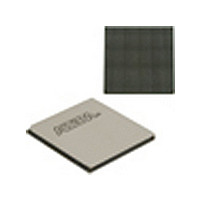
EP4SGX530HH35C2N Altera, EP4SGX530HH35C2N Datasheet - Page 7

EP4SGX530HH35C2N
Manufacturer Part Number
EP4SGX530HH35C2N
Description
IC STRATIX IV FPGA 530K 1152HBGA
Manufacturer
Altera
Series
Stratix® IV GXr
Datasheets
1.EP4SGX110DF29C3N.pdf
(80 pages)
2.EP4SGX110DF29C3N.pdf
(1154 pages)
3.EP4SGX110DF29C3N.pdf
(432 pages)
4.EP4SGX110DF29C3N.pdf
(22 pages)
5.EP4SGX110DF29C3N.pdf
(30 pages)
6.EP4SGX110DF29C3N.pdf
(72 pages)
7.EP4SGX530HH35C2N.pdf
(1145 pages)
Specifications of EP4SGX530HH35C2N
Number Of Logic Elements/cells
531200
Number Of Labs/clbs
21248
Total Ram Bits
27376
Number Of I /o
564
Voltage - Supply
0.87 V ~ 0.93 V
Mounting Type
Surface Mount
Operating Temperature
0°C ~ 85°C
Package / Case
1152-HBGA
Family Name
Stratix® IV
Number Of Logic Blocks/elements
531200
# Registers
424960
# I/os (max)
560
Process Technology
40nm
Operating Supply Voltage (typ)
900mV
Logic Cells
531200
Ram Bits
28033024
Operating Supply Voltage (min)
0.87V
Operating Supply Voltage (max)
0.93V
Operating Temp Range
0C to 85C
Operating Temperature Classification
Commercial
Mounting
Surface Mount
Pin Count
1152
Package Type
FCHBGA
Lead Free Status / RoHS Status
Lead free / RoHS Compliant
Number Of Gates
-
Lead Free Status / Rohs Status
Compliant
Available stocks
Company
Part Number
Manufacturer
Quantity
Price
Chapter 1: Overview for the Stratix IV Device Family
Architecture Features
February 2011 Altera Corporation
f
■
■
■
Diagnostic Features
■
■
■
For more information, refer to the
Signal Integrity
Stratix IV devices simplify the challenge of signal integrity through a number of chip,
package, and board-level enhancements to enable efficient high-speed data transfer
into and out of the device. These enhancements include:
■
■
■
■
■
■
XAUI/HiGig Support
■
■
■
GbE Support
■
■
■
Support for other protocol features such as MSB-to-LSB transmission in
SONET/SDH configuration and spread-spectrum clocking in PCIe configurations
Serial loopback from the transmitter serializer to the receiver CDR for transceiver
PCS and PMA diagnostics
Reverse serial loopback pre- and post-CDR to transmitter buffer for physical link
diagnostics
Loopback master and slave capability in PCI Express hard IP blocks
Programmable 3-tap transmitter pre-emphasis with up to 8,192 pre-emphasis
levels to compensate for pre-cursor and post-cursor inter-symbol interference (ISI)
Up to 900% boost capability on the first pre-emphasis post-tap
User-controlled and adaptive 4-stage receiver equalization with up to 16 dB of
high-frequency gain
On-die power supply regulators for transmitter and receiver phase-locked loop
(PLL) charge pump and voltage controlled oscillator (VCO) for superior noise
immunity
On-package and on-chip power supply decoupling to satisfy transient current
requirements at higher frequencies, thereby reducing the need for on-board
decoupling capacitors
Calibration circuitry for transmitter and receiver on-chip termination (OCT)
resistors
Compliant to IEEE802.3ae specification
Embedded state machine circuitry to convert XGMII idle code groups (||I||)
to and from idle ordered sets (||A||, ||K||, ||R||) at the transmitter and
receiver, respectively
8B/10B encoder and decoder, receiver synchronization state machine, lane
deskew, and ± 100 ppm clock compensation circuitry
Compliant to IEEE802.3-2005 specification
Automatic idle ordered set (/I1/, /I2/) generation at the transmitter,
depending on the current running disparity
8B/10B encoder and decoder, receiver synchronization state machine, and
± 100 ppm clock compensation circuitry
PCI Express Compiler User
Stratix IV Device Handbook Volume 1
Guide.
1–7


