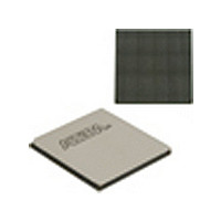
EP4SGX530HH35C2N Altera, EP4SGX530HH35C2N Datasheet - Page 8

EP4SGX530HH35C2N
Manufacturer Part Number
EP4SGX530HH35C2N
Description
IC STRATIX IV FPGA 530K 1152HBGA
Manufacturer
Altera
Series
Stratix® IV GXr
Datasheets
1.EP4SGX110DF29C3N.pdf
(80 pages)
2.EP4SGX110DF29C3N.pdf
(1154 pages)
3.EP4SGX110DF29C3N.pdf
(432 pages)
4.EP4SGX110DF29C3N.pdf
(22 pages)
5.EP4SGX110DF29C3N.pdf
(30 pages)
6.EP4SGX110DF29C3N.pdf
(72 pages)
7.EP4SGX530HH35C2N.pdf
(1145 pages)
Specifications of EP4SGX530HH35C2N
Number Of Logic Elements/cells
531200
Number Of Labs/clbs
21248
Total Ram Bits
27376
Number Of I /o
564
Voltage - Supply
0.87 V ~ 0.93 V
Mounting Type
Surface Mount
Operating Temperature
0°C ~ 85°C
Package / Case
1152-HBGA
Family Name
Stratix® IV
Number Of Logic Blocks/elements
531200
# Registers
424960
# I/os (max)
560
Process Technology
40nm
Operating Supply Voltage (typ)
900mV
Logic Cells
531200
Ram Bits
28033024
Operating Supply Voltage (min)
0.87V
Operating Supply Voltage (max)
0.93V
Operating Temp Range
0C to 85C
Operating Temperature Classification
Commercial
Mounting
Surface Mount
Pin Count
1152
Package Type
FCHBGA
Lead Free Status / RoHS Status
Lead free / RoHS Compliant
Number Of Gates
-
Lead Free Status / Rohs Status
Compliant
Available stocks
Company
Part Number
Manufacturer
Quantity
Price
1–8
Stratix IV Device Handbook Volume 1
FPGA Fabric and I/O Features
The following sections describe the Stratix IV FPGA fabric and I/O features.
Device Core Features
■
■
■
■
Embedded Memory
■
■
■
Digital Signal Processing (DSP) Blocks
■
■
■
Clock Networks
■
■
■
■
Up to 531,200 LEs in Stratix IV GX and GT devices and up to 813,050 LEs in
Stratix IV E devices, efficiently packed in unique and innovative adaptive logic
modules (ALMs)
Ten ALMs per logic array block (LAB) deliver faster performance, improved logic
utilization, and optimized routing
Programmable power technology, including a variety of process, circuit, and
architecture optimizations and innovations
Programmable power technology available to select power-driven compilation
options for reduced static power consumption
TriMatrix embedded memory architecture provides three different memory block
sizes to efficiently address the needs of diversified FPGA designs:
■
■
■
Up to 33,294 Kbit of embedded memory operating at up to 600 MHz
Each memory block is independently configurable to be a single- or dual-port
RAM, FIFO, ROM, or shift register
Flexible DSP blocks configurable as 9 × 9-bit, 12 × 12-bit, 18 × 18-bit, and
36 × 36-bit full-precision multipliers at up to 600 MHz with rounding and
saturation capabilities
Faster operation due to fully pipelined architecture and built-in addition,
subtraction, and accumulation units to combine multiplication results
Optimally designed to support advanced features such as adaptive filtering, barrel
shifters, and finite and infinite impulse response (FIR and IIR) filters
Up to 16 global clocks and 88 regional clocks optimally routed to meet the
maximum performance of 800 MHz
Up to 112 and 132 periphery clocks in Stratix IV GX and Stratix IV E devices,
respectively
Up to 66 (16 GCLK + 22 RCLK + 28 PCLK) clock networks per device quadrant in
Stratix IV GX and Stratix IV GT devices
Up to 71 (16 GCLK + 22 RCLK + 33 PCLK) clock networks per device quadrant in
Stratix IV E devices
640-bit MLAB
9-Kbit M9K
144-Kbit M144K
Chapter 1: Overview for the Stratix IV Device Family
February 2011 Altera Corporation
Architecture Features


