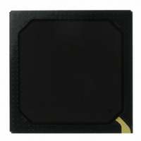
FWIXP425BD Intel, FWIXP425BD Datasheet - Page 34

FWIXP425BD
Manufacturer Part Number
FWIXP425BD
Description
IC NETWRK PROCESSR 533MHZ 492BGA
Manufacturer
Intel
Specifications of FWIXP425BD
Processor Type
Network
Features
XScale Core
Speed
533MHz
Voltage
1.3V
Mounting Type
Surface Mount
Package / Case
492-BGA
Lead Free Status / RoHS Status
Contains lead / RoHS non-compliant
Other names
852279
Available stocks
Company
Part Number
Manufacturer
Quantity
Price
Company:
Part Number:
FWIXP425BD
Manufacturer:
IDT
Quantity:
260
Part Number:
FWIXP425BD
Manufacturer:
INTEL/英特尔
Quantity:
20 000
Intel
Functional Signal Descriptions
Table 6.
Table 7.
34
®
IXP42X Product Line and IXC1100 Control Plane Processor
PCI Controller (Sheet 2 of 2)
High-Speed, Serial Interface 0
PCI_GNT_N[0]
PCI_INTA_N
PCI_CLKIN
†
HSS_TXFRAME0
HSS_TXDATA0
HSS_TXCLK0
HSS_RXFRAME0
HSS_RXDATA0
HSS_RXCLK0
For a legend of the Type codes, see
Name
Name
Reset
Reset
Power
Power
On
On
Z
Z
Z
Z
Z
Z
Z
Z
Z
†
†
Reset
Reset
VI
Z
Z
VI
Z
Z
Z
Z
Z
Table 4 on page
†
†
Type
Type
O/D
I/O
O/D
I
I/O
I/O
I/O
I/O
I
†
†
PCI arbitration grant:
Should be pulled high with a 10-KΩ resistor when not being utilized in the
system.
PCI interrupt: Used to request an interrupt.
Should be pulled high with a 10-KΩ resistor when not being utilized in the
system.
PCI Clock: provides timing for all transactions on PCI. All PCI signals —
except INTA#, INTB#, INTC#, and INTD# — are sampled on the rising edge of
CLK and timing parameters are defined with respect to this edge. The PCI
clock rate can operate at up to 66 MHz.
Should be pulled low with a 10-KΩ resistor when not being utilized in the
system.
30.
•
•
The High-Speed Serial (HSS) transmit frame signal can be configured as
an input or an output to allow an external source become synchronized
with the transmitted data. Often known as a Frame Sync signal.
Configured as an input upon reset.
Should be pulled low with a 10-KΩ resistor when not being utilized in the
system.
Transmit data out. Open Drain output.
Must be pulled high with a 10-KΩ resistor to V
The High-Speed Serial (HSS) transmit clock signal can be configured as an
input or an output. The clock can be a frequency ranging from 512 KHz to
8.192 MHz. Used to clock out the transmitted data. Configured as an input
upon reset. Frame sync and data can be selected to be generated on the
rising or falling edge of the transmit clock.
Should be pulled low with a 10-KΩ resistor when not being utilized in the
system.
The High-Speed Serial (HSS) receive frame signal can be configured as
an input or an output to allow an external source to become
synchronized with the received data. Often known as a Frame Sync
signal. Configured as an input upon reset.
Should be pulled low with a 10-KΩ resistor when not being utilized in the
system.
Receive data input. Can be sampled on the rising or falling edge of the
receive clock.
Should be pulled low through a 10-KΩ resistor when not being utilized in
the system.
The High-Speed Serial (HSS) receive clock signal can be configured as
an input or an output. The clock can be from 512 KHz to 8.192 MHz.
Used to sample the received data. Configured as an input upon reset.
Should be pulled low with a 10-KΩ resistor when not being utilized in the
system.
When configured as an output (PCI arbiter enabled), the internal PCI
arbiter to allow an agent to claim control of the PCI bus.
When configured as an input (PCI arbiter disabled), the pin will be
used to claim access of the PCI bus from an external arbiter.
Description
Description
CCP
.
Datasheet


