CS4202-JQZ Cirrus Logic Inc, CS4202-JQZ Datasheet - Page 19
CS4202-JQZ
Manufacturer Part Number
CS4202-JQZ
Description
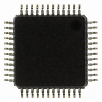
IC AC 97 W/HEADPHONE AMP 48TQFP
Manufacturer
Cirrus Logic Inc
Type
Audio Codec '97r
Datasheet
1.CS4202-JQZ.pdf
(66 pages)
Specifications of CS4202-JQZ
Package / Case
48-LQFP
Data Interface
Serial
Resolution (bits)
18, 20 b
Number Of Adcs / Dacs
1 / 1
Sigma Delta
Yes
Dynamic Range, Adcs / Dacs (db) Typ
90 / 90
Voltage - Supply, Analog
4.75 V ~ 5.25 V
Voltage - Supply, Digital
4.75 V ~ 5.25 V
Operating Temperature
0°C ~ 70°C
Mounting Type
Surface Mount
Number Of Adc Inputs
8
Number Of Dac Outputs
3
Conversion Rate
48 KSPS
Interface Type
Serial (5-Wire, I2S)
Resolution
18 bit, 20 bit
Operating Supply Voltage
3.3 V, 5 V
Maximum Operating Temperature
+ 70 C
Mounting Style
SMD/SMT
Minimum Operating Temperature
0 C
Number Of Channels
1 ADC/1 DAC
Supply Current
10 mA
Thd Plus Noise
- 84 dB
Lead Free Status / RoHS Status
Lead free / RoHS Compliant
Lead Free Status / RoHS Status
Lead free / RoHS Compliant, Lead free / RoHS Compliant
Other names
598-1181
Available stocks
Company
Part Number
Manufacturer
Quantity
Price
Company:

Part Number:
CS4202-JQZ
Manufacturer:
CIRRUS
Quantity:
800
Company:
Part Number:
CS4202-JQZ
Manufacturer:
IDT
Quantity:
388
Part Number:
CS4202-JQZ
Manufacturer:
CIRRUS
Quantity:
20 000
Company:
Part Number:
CS4202-JQZR
Manufacturer:
Cirrus Logic Inc
Quantity:
10 000


3.2.3 Status Data Port (Slot 2)
RD[15:0]
3.2.4 PCM Capture Data (Slot 3-4,6-8,11)
CD[17:0]
3.2.5 GPIO Pin Status (Slot 12)
GPIO[4:0]
BDI
GPIO_INT
DS549PP2
Bit 19 18
Bit 19
Bit 19
RD15 RD14 RD13 RD12 RD11 RD10 RD9 RD8 RD7 RD6 RD5 RD4 RD3 RD2 RD1 RD0
CD17 CD16 CD15 CD14 CD13 CD12 CD11 CD10 CD9 CD8 CD7 CD6 CD5 CD4 CD3 CD2 CD1 CD0
0
0
18
18
17
0
17
17
16
0
16
16
data will only be valid when the respective slot valid bit is ‘set’ in input Slot 0. The mapping of
a given slot to an ADC is determined by the state of the ASA[1:0] bits in the AC Mode Control
Register (index 5Eh). The definition of each slot can be found in Table 8 on page 30.
GPIO Pin Status. The GPIO[4:0] bits reflect the status of the CS4202 GPIO pins configured
as inputs. The pin status of GPIO pins configured as outputs will be reflected back on the
GPIO[4:0] bits of input Slot 12 in the next frame. The output GPIO pins are controlled by the
GPIO[4:0] pin control bits in output Slot 12.
BIOS-Driver Interface. The BDI bit indicates that a BIOS event has occurred. This bit is a logic
OR of all bits in the BDI Status Register (Index 7Ah) ANDed with their corresponding bit in the
BDI Config Register (Index 70h).
GPIO Interrupt. The GPIO_INT bit indicates that a GPIO or BDI interrupt event has occurred.
The occurrence of a BDI interrupt is determined by the BDI interrupt requirements as outlined
Read Data. The RD[15:0] bits contain the register data requested by the controller from the
previous read request. All read requests will return the read address in the input Slot 1 and
the register data in the input Slot 2 on the following serial data frame.
Capture Data. The CD [17:0] bits contain 18-bit PCM (2’s complement) capture data. The
The occurrence of a GPIO interrupt is determined by the GPIO interrupt requirements as out-
lined in the GPIO Pin Wakeup Mask Register (Index 52h) description. In this case, the
GPIO_INT bit is cleared by writing a ‘0’ to the bit in the GPIO Pin Status Register (Index 54h)
corresponding to the GPIO pin which generated the interrupt.
in the BDI Control Registers (Index 70h - 72h). In this case, the GPIO_INT bit is cleared by
writing a ‘0’ to the bit in the BDI Status Register (Index 7Ah) that generated the interrupt.
15
0
15
15
14
0
14
13
0
14
13
12
0
13
12
11
0
12
11
10
0
11
10
9
0
10
GPIO4 GPIO3 GPIO2 GPIO1 GPIO0 Res BDI Res
9
8
9
8
7
8
7
6
7
6
6
5
5
5
4
4
4
3
3
3
2
2
Reserved
CS4202
2
1
0
1
1
GPIO
_INT
0
0
0
0
19
Related parts for CS4202-JQZ
Image
Part Number
Description
Manufacturer
Datasheet
Request
R

Part Number:
Description:
IC AC97 W/Headphone Amplifier
Manufacturer:
Cirrus Logic Inc
Datasheet:
Part Number:
Description:
Development Kit
Manufacturer:
Cirrus Logic Inc
Datasheet:
Part Number:
Description:
Development Kit
Manufacturer:
Cirrus Logic Inc
Datasheet:


Part Number:
Description:
High-efficiency PFC + Fluorescent Lamp Driver Reference Design
Manufacturer:
Cirrus Logic Inc
Datasheet:
Part Number:
Description:
Development Kit
Manufacturer:
Cirrus Logic Inc
Datasheet:
Part Number:
Description:
Development Kit
Manufacturer:
Cirrus Logic Inc
Datasheet:

Part Number:
Description:
Development Kit
Manufacturer:
Cirrus Logic Inc
Datasheet:
Part Number:
Description:
Development Kit
Manufacturer:
Cirrus Logic Inc
Datasheet:
Part Number:
Description:
Development Kit
Manufacturer:
Cirrus Logic Inc
Datasheet:
Part Number:
Description:
Development Kit
Manufacturer:
Cirrus Logic Inc
Datasheet:
Part Number:
Description:
Development Kit
Manufacturer:
Cirrus Logic Inc
Datasheet:

Part Number:
Description:
Ref Bd For Speakerbar MSA & DSP Products
Manufacturer:
Cirrus Logic Inc