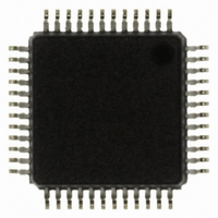
CS4202-JQZ Cirrus Logic Inc, CS4202-JQZ Datasheet - Page 39

CS4202-JQZ
Manufacturer Part Number
CS4202-JQZ
Description
IC AC 97 W/HEADPHONE AMP 48TQFP
Manufacturer
Cirrus Logic Inc
Type
Audio Codec '97r
Datasheet
1.CS4202-JQZ.pdf
(66 pages)
Specifications of CS4202-JQZ
Package / Case
48-LQFP
Data Interface
Serial
Resolution (bits)
18, 20 b
Number Of Adcs / Dacs
1 / 1
Sigma Delta
Yes
Dynamic Range, Adcs / Dacs (db) Typ
90 / 90
Voltage - Supply, Analog
4.75 V ~ 5.25 V
Voltage - Supply, Digital
4.75 V ~ 5.25 V
Operating Temperature
0°C ~ 70°C
Mounting Type
Surface Mount
Number Of Adc Inputs
8
Number Of Dac Outputs
3
Conversion Rate
48 KSPS
Interface Type
Serial (5-Wire, I2S)
Resolution
18 bit, 20 bit
Operating Supply Voltage
3.3 V, 5 V
Maximum Operating Temperature
+ 70 C
Mounting Style
SMD/SMT
Minimum Operating Temperature
0 C
Number Of Channels
1 ADC/1 DAC
Supply Current
10 mA
Thd Plus Noise
- 84 dB
Lead Free Status / RoHS Status
Lead free / RoHS Compliant
Lead Free Status / RoHS Status
Lead free / RoHS Compliant, Lead free / RoHS Compliant
Other names
598-1181
Available stocks
Company
Part Number
Manufacturer
Quantity
Price
Company:
Part Number:
CS4202-JQZ
Manufacturer:
CIRRUS
Quantity:
800
Company:
Part Number:
CS4202-JQZ
Manufacturer:
IDT
Quantity:
388
Part Number:
CS4202-JQZ
Manufacturer:
CIRRUS
Quantity:
20 000
Company:
Part Number:
CS4202-JQZR
Manufacturer:
Cirrus Logic Inc
Quantity:
10 000
4.25
SDEN
SDO2
SDSC
SDF[1:0]
Default
DS549PP2
SDEN
D15
Serial Port Control Register (Index 6Ah)
D14
0
D13
0
Serial Data Output Enable. The SDEN bit enables transmission of serial data on the SDOUT
pin. The SDEN bit routes the left and right channel data from the AC ’97 controller to the serial
data port. The actual data routed to the serial data port are controlled through the DSA[1:0]
configuration in the Extended Audio ID Register (Index 28h). SDEN also functions as a mas-
ter control for the second serial data output port and the serial clock. Setting this bit also dis-
ables the GPIO[1:0] pins and clears the GC[1:0] bits in the GPIO Pin Configuration Register
(Index 4Ch). Clearing this bit re-enables the GPIO[1:0] pins and sets the GC[1:0] bits.
Serial Data Output 2 Enable. The SDO2 bit enables transmission of serial data on the
GPIO4/SDO2 pin. The SDO2 bit routes the left and right channel data from the AC ’97 con-
troller to the second serial data port. The actual slots routed to the second serial data port are
controlled through the DSA[1:0] configuration in the Extended Audio ID Register (Index 28h).
This bit can only be ‘set’ if the SDEN bit is ‘1’ and will be ‘cleared’ automatically if SDEN re-
turns to ‘0’. Setting this bit also disables the GPIO4 pin and clears the GC4 bit in the GPIO
Pin Configuration Register (Index 4Ch). Clearing this bit re-enables the GPIO4 pin and sets
the GC4 bit.
Serial Clock Enable. The SDSC bit enables transmission of a serial clock on the EAPD/SCLK
pin. Serial data can be routed to DACs that support internal SCLK mode without transmitting
a serial clock. For DACs that only support external SCLK mode, transmission of a serial clock
is required and this bit must be set to ‘1’. This bit can only be set if the SDEN bit is ‘1’ and will
be cleared automatically if SDEN returns to ‘0’. Furthermore, the SDSC bit can only be ‘set’
if the EAPD bit in the Powerdown Control/Status Register (Index 26h) is ‘0’. If the SDEN bit
is ‘0’ or the EAPD bit is ‘1’, SDSC is a read-only bit and always returns ‘0’.
Serial Data Format. The SDF[1:0] bits control the format of the serial data transmitted on the
two output ports. All ports will use the same format. See Table 12 for available formats.
0000h
D12
0
D11
0
SDF1 SDF0
D10
Table 12. Serial Data Format Selection
0
0
0
1
1
D9
0
0
1
0
1
Right Justified, 20-bit data
Right Justified, 16-bit data
D8
0
Serial Data Format
Left Justified
D7
0
I
2
S
D6
0
D5
0
D4
0
SDO2 SDSC SDF1 SDF0
D3
D2
CS4202
D1
D0
39


