TDA8024T/C1,118 NXP Semiconductors, TDA8024T/C1,118 Datasheet - Page 11
TDA8024T/C1,118
Manufacturer Part Number
TDA8024T/C1,118
Description
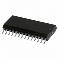
IC SMART CARD INTERFACE 28-SOIC
Manufacturer
NXP Semiconductors
Datasheet
1.TDA8024TTC1118.pdf
(29 pages)
Specifications of TDA8024T/C1,118
Package / Case
28-SOIC (7.5mm Width)
Controller Type
Smart Card Interface
Interface
Analog
Voltage - Supply
2.7 V ~ 6.5 V
Current - Supply
1.5mA
Operating Temperature
-25°C ~ 85°C
Mounting Type
Surface Mount
Maximum Operating Temperature
+ 85 C
Minimum Operating Temperature
- 25 C
Mounting Style
SMD/SMT
Lead Free Status / RoHS Status
Lead free / RoHS Compliant
Lead Free Status / RoHS Status
Lead free / RoHS Compliant, Lead free / RoHS Compliant
Other names
935271342118
TDA8024TD-T
TDA8024TD-T
TDA8024TD-T
TDA8024TD-T
Available stocks
Company
Part Number
Manufacturer
Quantity
Price

Part Number:
TDA8024T/C1,118
Manufacturer:
NXP/恩智浦
Quantity:
20 000


Philips Semiconductors
8.5
After a Power-on reset, the circuit enters the inactive
mode. A minimum number of circuits are active while
waiting for the microcontroller to start a session:
8.6
After power-on and after the internal pulse width delay, the
system microcontroller can check the presence of a card
using the signals OFF and CMDVCC as shown in Table 2.
2004 July 12
All card contacts are inactive (approximately 200
GND)
Pins I/OUC, AUX1UC and AUX2UC are in the
high-impedance state (11 k pull-up resistor to V
Voltage generators are stopped
XTAL oscillator is running
Voltage supervisor is active
The internal oscillator is running at its low frequency.
IC card interface
(1) Current.
(2) Voltage.
Fig.6
(V)
V o
6
4
2
0
Inactive mode
Activation sequence
0
I/O, AUX1 and AUX2 output voltage and
current as functions of time during a
LOW-to-HIGH transition.
(1)
20
40
(2)
t (ns)
FCE661
60
12
8
4
0
(mA)
I o
DD
)
to
11
Table 2 Card presence indication
If the card is in the reader (this is the case if PRES or
PRES is active), the system microcontroller can start a
card session by pulling CMDVCC LOW. The following
sequence then occurs (see Fig.6):
1. CMDVCC is pulled LOW and the internal oscillator
2. The voltage doubler is started (between t
3. V
4. I/O, AUX1 and AUX2 are enabled (t
5. CLK is applied to the C3 contact of the card reader (t
6. RST is enabled (t
The clock may be applied to the card using the following
sequence:
1. Set RSTIN HIGH.
2. Set CMDVCC LOW.
3. Reset RSTIN LOW between t
4. RST remains LOW until t
5. After t
If the applied clock is not needed, then CMDVCC may be
set LOW with RSTIN LOW. In this case, CLK will start at t
(minimum 200 ns after the transition on I/O), and after t
RSTIN may be set HIGH in order to obtain an Answer To
Request (ATR) from the card.
Activation should not be performed with RSTIN held
permanently HIGH.
changes to its high frequency (t
(t
internal oscillator (approximately 25 s).
were pulled LOW until this moment).
this moment.
the copy of RSTIN.
allows a precise count of CLK pulses before toggling
RST.
2
CC
HIGH
= t
LOW
OFF
rises from 0 to 5 V (or 3 V) with a controlled slope
1
5
, RSTIN has no further affect on CLK; this
+ 1.5
T) where T is 64 times the period of the
5
= t
CMDVCC
1
HIGH
HIGH
+ 7T).
5
, when RST is enabled to be
3
and t
0
).
Product specification
3
card present
card not present
5
; CLK will start at
= t
TDA8024
INDICATION
1
0
+ 4T) (these
and t
1
).
5
4
,
).
3
Related parts for TDA8024T/C1,118
Image
Part Number
Description
Manufacturer
Datasheet
Request
R

Part Number:
Description:
Manufacturer:
NXP Semiconductors
Datasheet:

Part Number:
Description:
IC SMART CARD INTERFACE 28-SOIC
Manufacturer:
NXP Semiconductors
Datasheet:
Part Number:
Description:
NXP Semiconductors designed the LPC2420/2460 microcontroller around a 16-bit/32-bitARM7TDMI-S CPU core with real-time debug interfaces that include both JTAG andembedded trace
Manufacturer:
NXP Semiconductors
Datasheet:

Part Number:
Description:
NXP Semiconductors designed the LPC2458 microcontroller around a 16-bit/32-bitARM7TDMI-S CPU core with real-time debug interfaces that include both JTAG andembedded trace
Manufacturer:
NXP Semiconductors
Datasheet:
Part Number:
Description:
NXP Semiconductors designed the LPC2468 microcontroller around a 16-bit/32-bitARM7TDMI-S CPU core with real-time debug interfaces that include both JTAG andembedded trace
Manufacturer:
NXP Semiconductors
Datasheet:
Part Number:
Description:
NXP Semiconductors designed the LPC2470 microcontroller, powered by theARM7TDMI-S core, to be a highly integrated microcontroller for a wide range ofapplications that require advanced communications and high quality graphic displays
Manufacturer:
NXP Semiconductors
Datasheet:
Part Number:
Description:
NXP Semiconductors designed the LPC2478 microcontroller, powered by theARM7TDMI-S core, to be a highly integrated microcontroller for a wide range ofapplications that require advanced communications and high quality graphic displays
Manufacturer:
NXP Semiconductors
Datasheet:
Part Number:
Description:
The Philips Semiconductors XA (eXtended Architecture) family of 16-bit single-chip microcontrollers is powerful enough to easily handle the requirements of high performance embedded applications, yet inexpensive enough to compete in the market for hi
Manufacturer:
NXP Semiconductors
Datasheet:
Part Number:
Description:
The XA-S3 device is a member of Philips Semiconductors? XA(eXtended Architecture) family of high performance 16-bitsingle-chip microcontrollers
Manufacturer:
NXP Semiconductors
Datasheet:

Part Number:
Description:
The NXP BlueStreak LH75401/LH75411 family consists of two low-cost 16/32-bit System-on-Chip (SoC) devices
Manufacturer:
NXP Semiconductors
Datasheet:
Part Number:
Description:
The NXP LPC3130/3131 combine an 180 MHz ARM926EJ-S CPU core, high-speed USB2
Manufacturer:
NXP Semiconductors
Datasheet:
Part Number:
Description:
The NXP LPC3141 combine a 270 MHz ARM926EJ-S CPU core, High-speed USB 2
Manufacturer:
NXP Semiconductors
Part Number:
Description:
The NXP LPC3143 combine a 270 MHz ARM926EJ-S CPU core, High-speed USB 2
Manufacturer:
NXP Semiconductors