TDA8024T/C1,118 NXP Semiconductors, TDA8024T/C1,118 Datasheet - Page 22
TDA8024T/C1,118
Manufacturer Part Number
TDA8024T/C1,118
Description
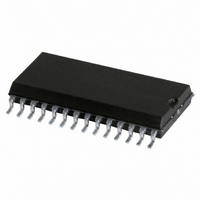
IC SMART CARD INTERFACE 28-SOIC
Manufacturer
NXP Semiconductors
Datasheet
1.TDA8024TTC1118.pdf
(29 pages)
Specifications of TDA8024T/C1,118
Package / Case
28-SOIC (7.5mm Width)
Controller Type
Smart Card Interface
Interface
Analog
Voltage - Supply
2.7 V ~ 6.5 V
Current - Supply
1.5mA
Operating Temperature
-25°C ~ 85°C
Mounting Type
Surface Mount
Maximum Operating Temperature
+ 85 C
Minimum Operating Temperature
- 25 C
Mounting Style
SMD/SMT
Lead Free Status / RoHS Status
Lead free / RoHS Compliant
Lead Free Status / RoHS Status
Lead free / RoHS Compliant, Lead free / RoHS Compliant
Other names
935271342118
TDA8024TD-T
TDA8024TD-T
TDA8024TD-T
TDA8024TD-T
Available stocks
Company
Part Number
Manufacturer
Quantity
Price

Part Number:
TDA8024T/C1,118
Manufacturer:
NXP/恩智浦
Quantity:
20 000


Philips Semiconductors
Notes
1. All parameters remain within limits but are tested only statistically for the temperature range. When a parameter is
2. If no external bridge is used then, to avoid any disturbance, it is recommended to connect pin 18 to ground. Pin 18
3. To meet these specifications, pin V
4. Permitted capacitor values are 100, or 100 + 100, or 220, or 220 + 100, or 330 nF.
5. Transition time and duty factor definitions are shown in Fig.12;
6. Pin CMDVCC is active LOW; pin RSTIN is active HIGH; for CLKDIV1 and CLKDIV2 functions see Table 1.
7. Pin PRES is active LOW; pin PRES is active HIGH; PRES has an integrated 1.25 A current source to GND
13 APPLICATION INFORMATION
Performance can be affected by the layout of the
application. For example, an additional cross-capacitance
of 1 pF between card reader contacts C2 and C3 or C2
and C7 can cause contact C2 to be polluted with high
frequency noise from C3 (or C7). In this case, include a
100 pF capacitor between contacts C2 and CGND.
Application recommendations:
2004 July 12
Ensure there is ample ground area around the TDA8024
and the connector; place the TDA8024 very near to the
connector; decouple the V
are best positioned under the connector)
The TDA8024 and the microcontroller must use the
same V
PRES, PRES, AUX1UC, I/OUC, AUX2UC, 5V/3V,
CMDVCC, and OFF are referred to V
to be driven by an external clock, also refer this pin to
V
IC card interface
handbook, full pagewidth
DD
specified as a function of V
is not connected in the TDA8024AT
ESR both with values of 100 nF, or one 100 nF and one 220 nF (see Fig.13).
(PRES to V
DD
supply. Pins CLKDIV1, CLKDIV2, RSTIN,
DD
); the card is considered present if at least one of the inputs PRES or PRES is active.
DD
DD
and V
Fig.12 Definition of output and input transition times.
or V
DDP
CC
CC
90%
DD
t r
lines (these lines
it means their actual value at the moment of measurement.
; if pin XTAL1 is
should be decoupled to CGND using two ceramic multilayer capacitors of low
10%
t 1
10%
90%
t f
22
With all these layout precautions, noise should be kept to
an acceptable level and jitter on C3 should be less than
100 ps.
Reference layouts are provided in “Application
note 10141” , available on request.
Track C3 should be placed as far as possible from the
other tracks
The track connecting CGND to C5 should be straight
(the two capacitors on C1 should be connected to this
ground track)
Avoid ground loops between CGND, PGND and GND
Decouple V
are the same in the application, then they should be
connected in star on the main track.
t 2
=
-------------- -
t
1
t
+
1
DDP
t
2
and V
V OH
V OH
V OL
DD
MDB058
2
V OL
separately; if the two supplies
Product specification
TDA8024
Related parts for TDA8024T/C1,118
Image
Part Number
Description
Manufacturer
Datasheet
Request
R

Part Number:
Description:
Manufacturer:
NXP Semiconductors
Datasheet:

Part Number:
Description:
IC SMART CARD INTERFACE 28-SOIC
Manufacturer:
NXP Semiconductors
Datasheet:
Part Number:
Description:
NXP Semiconductors designed the LPC2420/2460 microcontroller around a 16-bit/32-bitARM7TDMI-S CPU core with real-time debug interfaces that include both JTAG andembedded trace
Manufacturer:
NXP Semiconductors
Datasheet:

Part Number:
Description:
NXP Semiconductors designed the LPC2458 microcontroller around a 16-bit/32-bitARM7TDMI-S CPU core with real-time debug interfaces that include both JTAG andembedded trace
Manufacturer:
NXP Semiconductors
Datasheet:
Part Number:
Description:
NXP Semiconductors designed the LPC2468 microcontroller around a 16-bit/32-bitARM7TDMI-S CPU core with real-time debug interfaces that include both JTAG andembedded trace
Manufacturer:
NXP Semiconductors
Datasheet:
Part Number:
Description:
NXP Semiconductors designed the LPC2470 microcontroller, powered by theARM7TDMI-S core, to be a highly integrated microcontroller for a wide range ofapplications that require advanced communications and high quality graphic displays
Manufacturer:
NXP Semiconductors
Datasheet:
Part Number:
Description:
NXP Semiconductors designed the LPC2478 microcontroller, powered by theARM7TDMI-S core, to be a highly integrated microcontroller for a wide range ofapplications that require advanced communications and high quality graphic displays
Manufacturer:
NXP Semiconductors
Datasheet:
Part Number:
Description:
The Philips Semiconductors XA (eXtended Architecture) family of 16-bit single-chip microcontrollers is powerful enough to easily handle the requirements of high performance embedded applications, yet inexpensive enough to compete in the market for hi
Manufacturer:
NXP Semiconductors
Datasheet:
Part Number:
Description:
The XA-S3 device is a member of Philips Semiconductors? XA(eXtended Architecture) family of high performance 16-bitsingle-chip microcontrollers
Manufacturer:
NXP Semiconductors
Datasheet:

Part Number:
Description:
The NXP BlueStreak LH75401/LH75411 family consists of two low-cost 16/32-bit System-on-Chip (SoC) devices
Manufacturer:
NXP Semiconductors
Datasheet:
Part Number:
Description:
The NXP LPC3130/3131 combine an 180 MHz ARM926EJ-S CPU core, high-speed USB2
Manufacturer:
NXP Semiconductors
Datasheet:
Part Number:
Description:
The NXP LPC3141 combine a 270 MHz ARM926EJ-S CPU core, High-speed USB 2
Manufacturer:
NXP Semiconductors
Part Number:
Description:
The NXP LPC3143 combine a 270 MHz ARM926EJ-S CPU core, High-speed USB 2
Manufacturer:
NXP Semiconductors