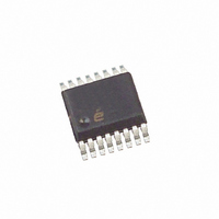
EL9110IUZ Intersil, EL9110IUZ Datasheet - Page 2

EL9110IUZ
Manufacturer Part Number
EL9110IUZ
Description
IC RECEIVR/EQUALIZER DIFF 16QSOP
Manufacturer
Intersil
Type
Receiverr
Datasheet
1.EL9110IUZ.pdf
(10 pages)
Specifications of EL9110IUZ
Number Of Drivers/receivers
0/1
Protocol
Twisted-Pair
Voltage - Supply
5V
Mounting Type
Surface Mount
Package / Case
16-QSOP
Device Type
Transceiver
Driver Case Style
QSOP
No. Of Pins
16
Operating Temperature Range
-40°C To +85°C
Filter Terminals
SMD
Transceiver Type
Differential
Rohs Compliant
Yes
Current Rating
60A
Frequency
150GHz
Lead Free Status / RoHS Status
Lead free / RoHS Compliant
Available stocks
Company
Part Number
Manufacturer
Quantity
Price
Part Number:
EL9110IUZ
Manufacturer:
INTERSIL
Quantity:
20 000
Company:
Part Number:
EL9110IUZ-T7
Manufacturer:
Intersil
Quantity:
2 000
Electrical Specifications
Absolute Maximum Ratings
Supply Voltage between V
Maximum Continuous Output Current . . . . . . . . . . . . . . . . . . . 30mA
Pin Voltages . . . . . . . . . . . . . . . . . . . . . . . . . V
CAUTION: Do not operate at or near the maximum ratings listed for extended periods of time. Exposure to such conditions may adversely impact product reliability and
result in failures not covered by warranty.
IMPORTANT NOTE: All parameters having Min/Max specifications are guaranteed. Typ values are for information purposes only. Unless otherwise noted, all tests are
at the specified temperature and are pulsed tests, therefore: T
AC PERFORMANCE
BW
SR
THD
DC PERFORMANCE
V
INPUT CHARACTERISTICS
CMIR
CMIRx
O
CMRR
CMRR+
CMBW
CM
C
R
C
R
+I
-I
V
OUTPUT CHARACTERISTICS
V
I
R
DiffGain
SUPPLY
I
I
PARAMETER
OUT
SON
SOFF
OS
IN
INDIFF
O
INDIFF
INDIFF
INCM
INCM
OUTCM
NOISE
IN
SLEW
Bandwidth
Slew Rate
Total Harmonic Distortion
Offset Voltage (bin #1)
Offset Voltage (bin #2)
Common-mode Input Range
Extended CMIR
Output Noise
Common-mode Rejection Ratio
Common-mode Rejection Ratio
CM Amplifier Bandwidth
CM Slew Rate
Differential Input Capacitance
Differential Input Resistance
CM Input Capacitance
CM Input Resistance
Positive Input Current
Negative Input Current
Differential Input Range
Output Voltage Swing
Output Drive Current
CM Output Resistance
Differential Gain
Supply Current
Supply Current
S
DESCRIPTION
+ and V
2
V
S
SA
- . . . . . . . . . . . . . . . . . . . . .12V
(T
+ = V
A
= +25°C)
A
S
+ = +5V, V
- -0.5V to V
Measured at 10kHz
Measured at 10MHz
R
V
V
V
J
(See Figure 1)
V
10MHz 1V
X2 gain, no equalization
Common-mode extension off
Common-mode extension on
V
10K || 10pF load
Measured @ +1V to -1V
Capacitance V
Resistance V
Capacitance V
Resistance V
DC bias @ V
DC bias @ V
V
R
V
at 100kHz
= T
IN
G
INP
L
L
G
C
ENBL
ENBL
SA
= 150Ω
= 10Ω, V
= 0, V
= 0.35, X2 gain, 75 + 75Ω load, V
= 0.35
= -1V to +1V, V
C
S
- = V
- V
+ +0.5V
= T
= 5, V
= 0, V
INM
A
G
A
P-P
- = -5V, T
= 0.35, X2 = 5, R
INP
when slope gain falls to 0.9
EL9110
INP
INP
INP
INP
INM
INM
out, V
INP
INP
= 1V, V
= V
= V
to V
= V
= 0
= 0
CONDITIONS
to V
= V
G
A
G
INM
INM
INM
= 0.35, V
INM
INM
= +25°C, Unless Otherwise Specified
= 0.35V, X2 gain, V
INM
INM
Thermal Information
Power Dissipation . . . . . . . . . . . . . . . . . . . . . . . . . . . . . See Curves
Storage Temperature . . . . . . . . . . . . . . . . . . . . . . . .-65°C to +150°C
Ambient Operating Temperature . . . . . . . . . . . . . . . .-40°C to +85°C
Die Junction Temperature . . . . . . . . . . . . . . . . . . . . . . . . . . . +150°C
Pb-free reflow profile . . . . . . . . . . . . . . . . . . . . . . . . . .see link below
= 0V
= 0V
to ground
http://www.intersil.com/pbfree/Pb-FreeReflow.asp
to ground
= 0V, X2 = gain,
L
C
= 75 + 75Ω
= 0, R
C
L
= 0.6
= 75 + 75Ω
C
= 0
(Note 1)
-250
0.85
MIN
2.5
0.4
50
27
1
1
CPI9049
-4/+3.5
TYP
±4.5
±3.5
150
100
600
-50
-10
1.5
2.4
1.2
2.8
3.2
1.0
25
60
50
50
60
30
1
1
(Note 1)
+250
MAX
1.1
0.8
38
November 30, 2007
FN7305.5
UNIT
RMS
MHz
MHz
V/ns
V/µs
dBc
MΩ
MΩ
mV
mV
mV
mA
mA
mA
dB
dB
pF
µA
µA
fF
Ω
V
V
V
V


