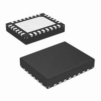
EL9111ILZ-T7 Intersil, EL9111ILZ-T7 Datasheet - Page 3

EL9111ILZ-T7
Manufacturer Part Number
EL9111ILZ-T7
Description
IC DIFF RCVR/EQUALZR TRPL 28-QFN
Manufacturer
Intersil
Type
Receiverr
Datasheet
1.EL9111ILZ.pdf
(13 pages)
Specifications of EL9111ILZ-T7
Number Of Drivers/receivers
0/3
Protocol
Twisted-Pair
Voltage - Supply
5V
Mounting Type
Surface Mount
Package / Case
28-VQFN
Lead Free Status / RoHS Status
Lead free / RoHS Compliant
Available stocks
Company
Part Number
Manufacturer
Quantity
Price
Company:
Part Number:
EL9111ILZ-T7
Manufacturer:
Intersil
Quantity:
98
Part Number:
EL9111ILZ-T7
Manufacturer:
INTERSIL
Quantity:
20 000
Electrical Specifications
Absolute Maximum Ratings
Supply Voltage between V
Maximum Continuous Output Current per Channel. . . . . . . . . 30mA
Power Dissipation . . . . . . . . . . . . . . . . . . . . . . . . . . . . . See Curves
Pin Voltages . . . . . . . . . . . . . . . . . . . . . . . . . V
CAUTION: Stresses above those listed in “Absolute Maximum Ratings” may cause permanent damage to the device. This is a stress only rating and operation of the
device at these or any other conditions above those indicated in the operational sections of this specification is not implied.
IMPORTANT NOTE: All parameters having Min/Max specifications are guaranteed. Typ values are for information purposes only. Unless otherwise noted, all tests are
at the specified temperature and are pulsed tests, therefore: T
AC PERFORMANCE
BW
SR
THD
DC PERFORMANCE
V(V
ΔV
INPUT CHARACTERISTICS
CMIR
O
CMRR
CMRR
CMBW
CM
C
R
C
R
+I
-I
V
OUTPUT CHARACTERISTICS
V(V
I(V
R(V
Gain
PARAMETER
IN
INDIFF
INDIFF
INDIFF
INCM
INCM
NOISE
IN
OS
OUT
SLEW
OUT
OUT
CM
)
)
)
)
OS
Bandwidth
Slew Rate
Total Harmonic Distortion
Offset Voltage
Channel-to-Channel Offset
Matching
Common-mode Input Range
Output Noise
Common-mode Rejection Ratio
Common-mode Rejection Ratio
CM Amplifier Bandwidth
CM Slew Rate
Differential Input Capacitance
Differential Input Resistance
CM Input Capacitance
CM Input Resistance
Positive Input Current
Negative Input Current
Differential Input Range
Output Voltage Swing
Output Drive Current
CM Output Resistance of
VCM_R/G/B (EL9112 only)
Gain
DESCRIPTION
S
+ and V
3
V
S
SA
- . . . . . . . . . . . . . . . . . . . . .12V
(T
+ = V
A
= +25°C)
A
+ = +5V, V
S
- -0.5V to V
(See Figure 1)
V
R
10MHz 2V
gain, V
X2 = high, no equalization
X2 = high, no equalization
V
R
10MHz
Measured at 10kHz
Measured at 10MHz
10k||10pF load
Measured @ +1V to -1V
Capacitance V
Resistance V
Capacitance V
Resistance V
DC
DC
V
to 0.9
R
R
X2 = high, V
at 100kHz
V
150Ω
IN
G
INP
C
L
LOAD
L
L
J
BIAS
BIAS
= T
= 75 + 75Ω
= 150Ω
= 10Ω, V
= 0, V
= 0V, V
SA
= -1V to +1V, V
- V
C
S
- = V
C
+ +0.5V
= 150Ω, Input 50Ω to GND,
= T
EL9111, EL9112
@ V
INM
@ V
= 0
G
CONDITIONS
P-P
A
C
A
= 0.39, X2 = 5, R
INP
G
- = -5V, T
when slope gain falls
INP
INP
= 0V, X2 = HIGH,
INP
INP
out, V
INP
INP
= 0.39
= 1V, V
= V
= V
to V
= V
G
to V
= V
INM
G
INM
= 0.39, V
INM
INM
A
INM
= 1V, X2
INM
INM
= +25°C, exposed die plate = -5V, unless otherwise specified.
= 0V
= 0V
to GND
Thermal Information
Storage Temperature . . . . . . . . . . . . . . . . . . . . . . . .-65°C to +150°C
Ambient Operating Temperature . . . . . . . . . . . . . . . .-40°C to +85°C
Die Junction Temperature . . . . . . . . . . . . . . . . . . . . . . . . . . . +150°C
Pb-free reflow profile . . . . . . . . . . . . . . . . . . . . . . . . . .see link below
to GND
= 0V,
http://www.intersil.com/pbfree/Pb-FreeReflow.asp
L
C
=
= 0,
-110
-100
0.85
MIN
2.5
50
1
1
-4 to
TYP
+3.5
-110
±3.5
150
100
600
-50
-10
-80
-55
1.5
2.4
1.2
2.8
3.2
1.0
50
60
30
0
1
1
MAX
+100
+78
1.1
May 9, 2007
FN7450.4
kV/µs
UNIT
MHz
dBm
MHz
V/µs
dBc
MΩ
MΩ
mV
mV
mA
dB
dB
pF
µA
µA
fF
V
V
V
Ω


