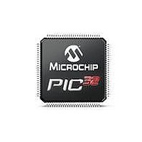
PIC32MX775F256H-80V/PT Microchip Technology, PIC32MX775F256H-80V/PT Datasheet - Page 153

PIC32MX775F256H-80V/PT
Manufacturer Part Number
PIC32MX775F256H-80V/PT
Description
256 KB Flash, 64 KB RAM, USB-OTG, Dual CAN, Ethernet, 80 MHz, 10-Bit ADC, DMA 64
Manufacturer
Microchip Technology
Series
PIC® 32MXr
Datasheet
1.PIC32MX575F256H-80VPT.pdf
(256 pages)
Specifications of PIC32MX775F256H-80V/PT
Processor Series
PIC32MX7xx
Core
MIPS
Data Bus Width
32 bit
Program Memory Type
Flash
Program Memory Size
256 KB
Data Ram Size
64 KB
Interface Type
USB, I2C, UART, RS-232, RS-485, SPI
Maximum Clock Frequency
80 MHz
Number Of Programmable I/os
5
Number Of Timers
5
Operating Supply Voltage
2.3 V to 3.6 V
Maximum Operating Temperature
+ 85 C
Mounting Style
SMD/SMT
Package / Case
TQFP-100
Operating Temperature Range
- 40 C to + 85 C
Supply Current (max)
10 mA
Core Processor
MIPS32® M4K™
Core Size
32-Bit
Speed
80MHz
Connectivity
CAN, Ethernet, I²C, SPI, UART/USART, USB OTG
Peripherals
Brown-out Detect/Reset, DMA, POR, PWM, WDT
Number Of I /o
53
Eeprom Size
-
Ram Size
64K x 8
Voltage - Supply (vcc/vdd)
2.3 V ~ 3.6 V
Data Converters
A/D 16x10b
Oscillator Type
Internal
Operating Temperature
-40°C ~ 105°C
Lead Free Status / Rohs Status
Details
Available stocks
Company
Part Number
Manufacturer
Quantity
Price
Company:
Part Number:
PIC32MX775F256H-80V/PT
Manufacturer:
Microchip Technology
Quantity:
10 000
- Current page: 153 of 256
- Download datasheet (6Mb)
22.0
The PIC32MX5XX/6XX/7XX 10-bit Analog-to-Digital
Converter (ADC) includes the following features:
• Successive Approximation Register (SAR)
• Up to 1 Msps conversion speed
• Up to 16 analog input pins
• External voltage reference input pins
FIGURE 22-1:
© 2009-2011 Microchip Technology Inc.
conversion
Note 1: This data sheet summarizes the features
Note
CH0SA<4:0>
2: Some registers and associated bits
10-BIT ANALOG-TO-DIGITAL
CONVERTER (ADC)
Channel
Scan
of the PIC32MX5XX/6XX/7XX family of
devices. It is not intended to be a
comprehensive reference source. To
complement the information in this data
sheet, refer to Section 17. “10-bit
Analog-to-Digital Converter (ADC)”
(DS61104)
Reference Manual” , which is available
from
(www.microchip.com/PIC32).
described in this section may not be
available on all devices. Refer to
Section 4.0 “Memory Organization”
this data sheet for device-specific register
and bit information.
1:
V
REFL
AN1
V
AN15
REF
AN0
CSCNA
CH0NA CH0NB
+ and V
the
ADC1 MODULE BLOCK DIAGRAM
CH0SB<4:0>
in
REF
Microchip
- inputs can be multiplexed with other analog inputs.
the
Input Selection
Alternate
“PIC32
web
+
-
Family
site
in
S/H
• One unipolar, differential Sample and Hold
• Automatic Channel Scan mode
• Selectable conversion trigger source
• 16-word conversion result buffer
• Selectable buffer fill modes
• Eight conversion result format options
• Operation during CPU Sleep and Idle modes
A block diagram of the 10-bit ADC is illustrated in
Figure
pins, designated AN0-AN15. In addition, there are two
analog input pins for external voltage reference
connections. These voltage reference inputs may be
shared with other analog input pins and may be
common to other analog module references.
The analog inputs are connected through two multi-
plexers (MUXs) to one SHA. The analog input MUXs
can be switched between two sets of analog inputs
between conversions. Unipolar differential conversions
are possible on all
the reference, using a reference input pin (see
Figure
The Analog Input Scan mode sequentially converts
user-specified channels. A control register specifies
which analog input channels will be included in the
scanning sequence.
The 10-bit ADC is connected to a 16-word result buffer.
Each 10-bit result is converted to one of eight 32-bit
output formats when it is read from the result buffer.
PIC32MX5XX/6XX/7XX
Amplifier (SHA)
V
REF
22-1. The 10-bit ADC has up to 16 analog input
22-1).
+
(1)
V
REFH
AV
VCFG<2:0>
SAR ADC
DD
V
channels,
REF
V
REFL
-
(1)
AV
other than the pin used as
SS
ADC1BUFE
ADC1BUF0
ADC1BUF1
ADC1BUF2
ADC1BUFF
DS61156G-page 153
Related parts for PIC32MX775F256H-80V/PT
Image
Part Number
Description
Manufacturer
Datasheet
Request
R

Part Number:
Description:
Manufacturer:
Microchip Technology Inc.
Datasheet:

Part Number:
Description:
Manufacturer:
Microchip Technology Inc.
Datasheet:

Part Number:
Description:
Manufacturer:
Microchip Technology Inc.
Datasheet:

Part Number:
Description:
Manufacturer:
Microchip Technology Inc.
Datasheet:

Part Number:
Description:
Manufacturer:
Microchip Technology Inc.
Datasheet:

Part Number:
Description:
Manufacturer:
Microchip Technology Inc.
Datasheet:

Part Number:
Description:
Manufacturer:
Microchip Technology Inc.
Datasheet:

Part Number:
Description:
Manufacturer:
Microchip Technology Inc.
Datasheet:


