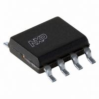
PCA9540BD,118 NXP Semiconductors, PCA9540BD,118 Datasheet - Page 4

PCA9540BD,118
Manufacturer Part Number
PCA9540BD,118
Description
IC I2C MUX 2CH 8-SOIC
Manufacturer
NXP Semiconductors
Datasheet
1.PCA9540BDP118.pdf
(22 pages)
Specifications of PCA9540BD,118
Package / Case
8-SOIC (3.9mm Width)
Applications
2-Channel I²C Multiplexer
Interface
I²C
Voltage - Supply
2.3 V ~ 3.6 V, 4.5 V ~ 5.5 V
Mounting Type
Surface Mount
Product
Decoders, Encoders, Multiplexers & Demultiplexers
Number Of Lines (input / Output)
2.0 / 1.0
Propagation Delay Time
0.3 ns at 2.3 V to 5.5 V
Supply Voltage (max)
5.5 V
Supply Voltage (min)
2.3 V
Maximum Operating Temperature
+ 85 C
Minimum Operating Temperature
- 40 C
Mounting Style
SMD/SMT
Number Of Input Lines
2.0
Number Of Output Lines
1.0
Lead Free Status / RoHS Status
Lead free / RoHS Compliant
For Use With
568-3615 - DEMO BOARD I2C
Lead Free Status / Rohs Status
Lead free / RoHS Compliant
Other names
568-1844-2
935276035118
PCA9540BD-T
935276035118
PCA9540BD-T
NXP Semiconductors
6. Functional description
PCA9540B_4
Product data sheet
6.2.1 Control register definition
6.1 Device addressing
6.2 Control register
Refer to
Following a START condition the bus master must output the address of the slave it is
accessing. The address of the PCA9540B is shown in
The last bit of the slave address defines the operation to be performed. When set to
logic 1 a read is selected, while a logic 0 selects a write operation.
Following the successful acknowledgement of the slave address, the bus master will send
a byte to the PCA9540B which will be stored in the Control register. If multiple bytes are
received by the PCA9540B, it will save the last byte received. This register can be written
and read via the I
A SCx/SDx downstream pair, or channel, is selected by the contents of the Control
register. This register is written after the PCA9540B has been addressed. The 2 LSBs of
the control byte are used to determine which channel is to be selected. When a channel is
selected, it will become active after a STOP condition has been placed on the I
This ensures that all SCx/SDx lines will be in a HIGH state when the channel is made
active, so that no false conditions are generated at the time of connection.
Fig 5.
Fig 6.
Figure 1 “Block diagram of
Slave address
Control register
2
C-bus.
Rev. 04 — 3 September 2009
7
X
1
X
6
1
PCA9540B”.
X
5
slave address
1
enable bit
X
4
fixed
0
X
3
0
channel selection bits
B2
2
0
(read/write)
B1
002aae717
1
002aae716
0
Figure
B0
0
R/W
2-channel I
5.
PCA9540B
2
C-bus multiplexer
© NXP B.V. 2009. All rights reserved.
2
C-bus.
4 of 22


