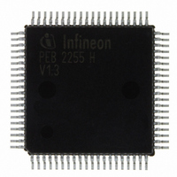
PEB2255H-V13 Infineon Technologies, PEB2255H-V13 Datasheet - Page 109

PEB2255H-V13
Manufacturer Part Number
PEB2255H-V13
Description
IC INTERFACE LINE 80-MQFP
Manufacturer
Infineon Technologies
Datasheet
1.PEB2255H-V13.pdf
(374 pages)
Specifications of PEB2255H-V13
Applications
*
Interface
*
Voltage - Supply
*
Package / Case
80-SQFP
Mounting Type
Surface Mount
Lead Free Status / RoHS Status
Lead free / RoHS Compliant
Other names
PEB2255H-V13
PEB2255H-V13IN
PEB2255H-V13IN
Available stocks
Company
Part Number
Manufacturer
Quantity
Price
Company:
Part Number:
PEB2255H-V13
Manufacturer:
Infineon Technologies
Quantity:
10 000
- Current page: 109 of 374
- Download datasheet (6Mb)
5.1.8
According to the input jitter defined by PUB62411 the FALC
jitter, which is specified in
Table 24
Specification
PUB 62411
5.1.9
The transmit jitter attenuator DCO-X circuitry generates a “jitter free“ transmit clock and
meets the following requirements: PUB 62411, PUB 43802, TR-TSY 009,TR-TSY 253,
TR-TSY 499 and ITU-T I.431 and G.703. The DCO-X circuitry works internally with the
same high frequency clock as the receive jitter attenuator it does. It synchronizes either
to the working clock of the transmit backplane interface or the clock provided by pin
SYNC2 (1.544 MHz if LIM1.DCOC=0 or 2.048 MHz if LIM1.DCOC=1) or the receive
clock RCLK (remote loop with JATT/loop-timed). The DCO-X attenuates the incoming
jitter starting at 6 Hz with 20 dB per decade fall off. With the jitter attenuated clock, which
is directly dependent on the phase difference of the incoming clock and the jitter
attenuated clock, data is read from the transmit elastic buffer (2 frames) or from the JATT
buffer (2 frames, remote loop with JATT) Wander with a jitter frequency below 6 Hz is
passed transparently.
The DCO-X accepts gapped clocks which are used in ATM or SDH/SONET applications.
The jitter attenuated clock is output on pin XCLK.
The transmit jitter attenuator can be disabled.
In the loop-timed clock configuration (LIM2.ELT) the DCO-X circuitry generates a
transmit clock which is frequency synchronized with RCLK. In this configuration the
transmit elastic buffer has to be enabled.
Data Sheet
Output Jitter (T1/J1)
Transmit Jitter Attenuator (T1/J1)
Output Jitter (T1/J1)
Lower Cutoff
10 Hz
8 kHz
10 Hz
Measurement Filter Bandwidth
Table 24Table
Broadband
109
below.
Upper Cutoff
8 kHz
40 kHz
40 kHz
Functional Description T1/J1
®
-LH generates the output
Output Jitter
(UI peak to peak)
< 0.02
< 0.02
< 0.02
< 0.02
FALC-LH V1.3
PEB 2255
2000-07
Related parts for PEB2255H-V13
Image
Part Number
Description
Manufacturer
Datasheet
Request
R

Part Number:
Description:
E1/t1/j1 Framer And Line Interface Component For Long And Short Haul Applications
Manufacturer:
Infineon Technologies Corporation
Datasheet:

Part Number:
Description:
Manufacturer:
Infineon Technologies AG
Datasheet:

Part Number:
Description:
Manufacturer:
Infineon Technologies AG
Datasheet:

Part Number:
Description:
Manufacturer:
Infineon Technologies AG
Datasheet:

Part Number:
Description:
Manufacturer:
Infineon Technologies AG
Datasheet:

Part Number:
Description:
Manufacturer:
Infineon Technologies AG
Datasheet:

Part Number:
Description:
Manufacturer:
Infineon Technologies AG
Datasheet:

Part Number:
Description:
Manufacturer:
Infineon Technologies AG
Datasheet:

Part Number:
Description:
16-bit microcontroller with 2x2 KByte RAM
Manufacturer:
Infineon Technologies AG
Datasheet:

Part Number:
Description:
NPN silicon RF transistor
Manufacturer:
Infineon Technologies AG
Datasheet:

Part Number:
Description:
NPN silicon RF transistor
Manufacturer:
Infineon Technologies AG
Datasheet:

Part Number:
Description:
NPN silicon RF transistor
Manufacturer:
Infineon Technologies AG
Datasheet:

Part Number:
Description:
NPN silicon RF transistor
Manufacturer:
Infineon Technologies AG
Datasheet:

Part Number:
Description:
Si-MMIC-amplifier in SIEGET 25-technologie
Manufacturer:
Infineon Technologies AG
Datasheet:

Part Number:
Description:
IGBT Power Module
Manufacturer:
Infineon Technologies AG
Datasheet:


