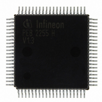
PEB2255H-V13 Infineon Technologies, PEB2255H-V13 Datasheet - Page 112

PEB2255H-V13
Manufacturer Part Number
PEB2255H-V13
Description
IC INTERFACE LINE 80-MQFP
Manufacturer
Infineon Technologies
Datasheet
1.PEB2255H-V13.pdf
(374 pages)
Specifications of PEB2255H-V13
Applications
*
Interface
*
Voltage - Supply
*
Package / Case
80-SQFP
Mounting Type
Surface Mount
Lead Free Status / RoHS Status
Lead free / RoHS Compliant
Other names
PEB2255H-V13
PEB2255H-V13IN
PEB2255H-V13IN
Available stocks
Company
Part Number
Manufacturer
Quantity
Price
Company:
Part Number:
PEB2255H-V13
Manufacturer:
Infineon Technologies
Quantity:
10 000
- Current page: 112 of 374
- Download datasheet (6Mb)
• Frame alignment between system frame and receive route frame
• Reporting and controlling of slips
Controlled by special signals generated by the receiver, the unipolar bit stream is
converted into bit-parallel, time slot serial data which is circularly written to the elastic
buffer using the internally generated Receive Route Clock (RCLK).
Reading of stored data is controlled by the System Clock sourced by SCLKR and the
Synchronous Pulse (SYPR) in conjunction with the programmed offset values for the
receive time slot/clock slot counters. After conversion into a serial data stream, the data
is given out via port RDO. If the receive buffer is bypassed, data is clocked off with RCLK
instead of SCLKR.
If 8.192 MHz reference frequency is used, one of two channel translation modes has to
be selected. The 24 received time slots (T1/J1) can be translated into the 32 system time
slots (E1) in two different channel translation modes (selected by FMR1.CTM).
Unequipped time slots are set to ‘FF
In one frame or short buffer mode the delay through the receive buffer is reduced to an
average delay of 96 or 48 bits. In this case SYPR to be programmed as input is not
allowed. Slips are performed in all buffer modes except the bypass mode. After a slip is
detected the read pointer is adjusted to one half of the current buffer size. The following
table gives an overview of the receive buffer operating mode.
•.
Table 25
SIC1.RBS1...0
11
10
01
00
1)
Data Sheet
In bypass mode the clock provided on pin SCLKR is ignored. Clocking is done with RCLK.
Receive Buffer Operating Modes (T1/J1)
Buffer Size
bypass
short buffer
1 frame
2 frames
1)
TS Offset programing (RC1...0)
RFM (SYPR = output) must be
selected; value of RC1...0
determines the position of RFM
RFM (SYPR = output) must be
selected; value of RC1...0
determines the position of RFM
RFM (SYPR = output) must be
selected; value of RC1...0
determines the position of RFM
SYPR is input and determines the
frame position together with
RC1...0 offset.
H
’. Refer to
112
Table
26.
Functional Description T1/J1
Slip
performance
no slips
yes
yes
yes
Slips are
performed on the
frame boundary
FALC-LH V1.3
PEB 2255
2000-07
Related parts for PEB2255H-V13
Image
Part Number
Description
Manufacturer
Datasheet
Request
R

Part Number:
Description:
E1/t1/j1 Framer And Line Interface Component For Long And Short Haul Applications
Manufacturer:
Infineon Technologies Corporation
Datasheet:

Part Number:
Description:
Manufacturer:
Infineon Technologies AG
Datasheet:

Part Number:
Description:
Manufacturer:
Infineon Technologies AG
Datasheet:

Part Number:
Description:
Manufacturer:
Infineon Technologies AG
Datasheet:

Part Number:
Description:
Manufacturer:
Infineon Technologies AG
Datasheet:

Part Number:
Description:
Manufacturer:
Infineon Technologies AG
Datasheet:

Part Number:
Description:
Manufacturer:
Infineon Technologies AG
Datasheet:

Part Number:
Description:
Manufacturer:
Infineon Technologies AG
Datasheet:

Part Number:
Description:
16-bit microcontroller with 2x2 KByte RAM
Manufacturer:
Infineon Technologies AG
Datasheet:

Part Number:
Description:
NPN silicon RF transistor
Manufacturer:
Infineon Technologies AG
Datasheet:

Part Number:
Description:
NPN silicon RF transistor
Manufacturer:
Infineon Technologies AG
Datasheet:

Part Number:
Description:
NPN silicon RF transistor
Manufacturer:
Infineon Technologies AG
Datasheet:

Part Number:
Description:
NPN silicon RF transistor
Manufacturer:
Infineon Technologies AG
Datasheet:

Part Number:
Description:
Si-MMIC-amplifier in SIEGET 25-technologie
Manufacturer:
Infineon Technologies AG
Datasheet:

Part Number:
Description:
IGBT Power Module
Manufacturer:
Infineon Technologies AG
Datasheet:


