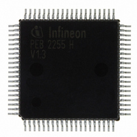
PEB2255H-V13 Infineon Technologies, PEB2255H-V13 Datasheet - Page 284

PEB2255H-V13
Manufacturer Part Number
PEB2255H-V13
Description
IC INTERFACE LINE 80-MQFP
Manufacturer
Infineon Technologies
Datasheet
1.PEB2255H-V13.pdf
(374 pages)
Specifications of PEB2255H-V13
Applications
*
Interface
*
Voltage - Supply
*
Package / Case
80-SQFP
Mounting Type
Surface Mount
Lead Free Status / RoHS Status
Lead free / RoHS Compliant
Other names
PEB2255H-V13
PEB2255H-V13IN
PEB2255H-V13IN
Available stocks
Company
Part Number
Manufacturer
Quantity
Price
Company:
Part Number:
PEB2255H-V13
Manufacturer:
Infineon Technologies
Quantity:
10 000
- Current page: 284 of 374
- Download datasheet (6Mb)
Transmit Control 1 (Read/Write)
Value after RESET: 00
XCOS…
XTO5…XTO0… Transmit Time Slot Offset
Receive Control 0 (Read/Write)
Value after RESET: 00
RCOS…
Data Sheet
RC0
XC1
RCOS
XCOS
7
7
A write access to this address resets the transmit elastic buffer to its
basic starting position. Therefore, updating of the value should only
be done when the FALC
be centered. As a consequence a transmit slip occurs.
Transmit Clock Offset Shift
Valid only if SIC1.SXSC = 0
0…
edge of SCLKX (after SYPX goes active) is an even number in the
range of 0 to 1022 SCLKX cycles.
1…
cycles.
Initial value loaded into the transmit bit counter at the trigger edge of
SCLKX when the synchronous pulse on port SYPX is active. Setting
of SIC1.SXSC enforces programming the offset values in the range
of 0 to 192 bits.
Receive Clock Offset
Valid only if SIC1.SXSC = 0
0
edge of SCLKR (after SYPX goes active) is an even number in the
range of 0 to 1022 SCLKX cycles.
1…
cycles.
SICS
H
H
The delay T between the beginning of time slot 0 and the initial
The delay T is an odd number in the range of 1 to 1023 SCLKX
The delay T is an odd number in the range of 1 to 1023 SCLKX
The delay T between the beginning of time slot 0 and the initial
XTO5
CRCI
XCRCI
XTO4
284
®
-LH is initialized or when the buffer should
XTO3
RDIS
RCO2
XTO2
RCO1
XTO1
FALC-LH V1.3
T1/J1 Registers
RCO0
XTO0
0
0
PEB 2255
2000-07
(21)
(22)
Related parts for PEB2255H-V13
Image
Part Number
Description
Manufacturer
Datasheet
Request
R

Part Number:
Description:
E1/t1/j1 Framer And Line Interface Component For Long And Short Haul Applications
Manufacturer:
Infineon Technologies Corporation
Datasheet:

Part Number:
Description:
Manufacturer:
Infineon Technologies AG
Datasheet:

Part Number:
Description:
Manufacturer:
Infineon Technologies AG
Datasheet:

Part Number:
Description:
Manufacturer:
Infineon Technologies AG
Datasheet:

Part Number:
Description:
Manufacturer:
Infineon Technologies AG
Datasheet:

Part Number:
Description:
Manufacturer:
Infineon Technologies AG
Datasheet:

Part Number:
Description:
Manufacturer:
Infineon Technologies AG
Datasheet:

Part Number:
Description:
Manufacturer:
Infineon Technologies AG
Datasheet:

Part Number:
Description:
16-bit microcontroller with 2x2 KByte RAM
Manufacturer:
Infineon Technologies AG
Datasheet:

Part Number:
Description:
NPN silicon RF transistor
Manufacturer:
Infineon Technologies AG
Datasheet:

Part Number:
Description:
NPN silicon RF transistor
Manufacturer:
Infineon Technologies AG
Datasheet:

Part Number:
Description:
NPN silicon RF transistor
Manufacturer:
Infineon Technologies AG
Datasheet:

Part Number:
Description:
NPN silicon RF transistor
Manufacturer:
Infineon Technologies AG
Datasheet:

Part Number:
Description:
Si-MMIC-amplifier in SIEGET 25-technologie
Manufacturer:
Infineon Technologies AG
Datasheet:

Part Number:
Description:
IGBT Power Module
Manufacturer:
Infineon Technologies AG
Datasheet:


