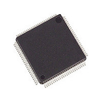
M30626FHPGP Renesas Electronics America, M30626FHPGP Datasheet - Page 28

M30626FHPGP
Manufacturer Part Number
M30626FHPGP
Description
Manufacturer
Renesas Electronics America
Datasheet
1.M30626FHPGP.pdf
(103 pages)
Specifications of M30626FHPGP
Cpu Family
M16C
Device Core Size
16/32Bit
Frequency (max)
24MHz
Interface Type
I2C/IEBus/UART
Program Memory Type
Flash
Program Memory Size
384KB
Total Internal Ram Size
31KB
# I/os (max)
87
Number Of Timers - General Purpose
11
Operating Supply Voltage (typ)
5V
Operating Supply Voltage (max)
5.5V
Operating Supply Voltage (min)
3.3V
On-chip Adc
26-chx10-bit
On-chip Dac
2-chx8-bit
Instruction Set Architecture
CISC
Operating Temp Range
-20C to 85C
Operating Temperature Classification
Commercial
Mounting
Surface Mount
Pin Count
100
Package Type
LQFP
Lead Free Status / Rohs Status
Compliant
Available stocks
Company
Part Number
Manufacturer
Quantity
Price
Company:
Part Number:
M30626FHPGP
Manufacturer:
RENESAS
Quantity:
24
Part Number:
M30626FHPGP
Manufacturer:
RENESAS/瑞萨
Quantity:
20 000
Company:
Part Number:
M30626FHPGP#U3C
Manufacturer:
Renesas
Quantity:
300
Company:
Part Number:
M30626FHPGP#U3C
Manufacturer:
Renesas
Quantity:
834
Company:
Part Number:
M30626FHPGP#U3C
Manufacturer:
Renesas Electronics America
Quantity:
10 000
Part Number:
M30626FHPGP#U5
Manufacturer:
RENESAS/瑞萨
Quantity:
20 000
Company:
Part Number:
M30626FHPGP#U5C
Manufacturer:
Renesas Electronics America
Quantity:
10 000
Part Number:
M30626FHPGP#U5C
Manufacturer:
RENESAS/瑞萨
Quantity:
20 000
Company:
Part Number:
M30626FHPGP#U7C
Manufacturer:
Renesas Electronics America
Quantity:
10 000
M16C/62P Group (M16C/62P, M16C/62PT)
Rev.2.41
REJ03B0001-0241
Table 1.18
I : Input
NOTES:
Main clock
input
Main clock
output
Sub clock input XCIN
Sub clock
output
BCLK output
Clock output
INT interrupt
input
NMI interrupt
input
Key input
interrupt input
Timer A
Timer B
Three-phase
motor control
output
Serial interface CTS0 to
I
2
Signal Name
C mode
1. When use VCC1 > VCC2, contacts due to some points or restrictions to be checked.
2. This pin function in M16C/62PT cannot be used.
3. Ask the oscillator maker the oscillation characteristic.
Jan 10, 2006
O : Output
(2)
Pin Description (100-pin and 128-pin Version) (2)
XIN
XOUT
XCOUT
BCLK
CLKOUT
INT0 to INT2
NT3 to INT5
NMI
KI0 to KI3
TA0OUT to
TA4OUT
TA0IN to
TA4IN
ZP
TB0IN to
TB5IN
U, U, V, V,
W, W
CTS2
RTS0 to
RTS2
CLK0 to
CLK4
RXD0 to
RXD2
SIN3, SIN4
TXD0 to
TXD2
SOUT3,
SOUT4
CLKS1
SDA0 to
SDA2
SCL0 to
SCL2
Pin Name
I/O : Input and output
Page 26 of 96
Type
I/O
I/O
I/O
I/O
I/O
O
O
O
O
O
O
O
O
O
I
I
I
I
I
I
I
I
I
I
I
I
Supply
Power
VCC1
VCC1
VCC1
VCC1
VCC2
VCC2
VCC1
VCC2
VCC1
VCC1
VCC1
VCC1
VCC1
VCC1
VCC1
VCC1
VCC1
VCC1
VCC1
VCC1
VCC1
VCC1
VCC1
VCC1
VCC1
(1)
I/O pins for the main clock generation circuit. Connect a ceramic
resonator or crystal oscillator between XIN and XOUT
the external clock, input the clock from XIN and leave XOUT open.
I/O pins for a sub clock oscillation circuit. Connect a crystal
oscillator between XCIN and XCOUT
input the clock from XCIN and leave XCOUT open.
Outputs the BCLK signal.
The clock of the same cycle as fC, f8, or f32 is outputted.
Input pins for the INT interrupt.
Input pin for the NMI interrupt. Pin states can be read by the P8_5
bit in the P8 register.
Input pins for the key input interrupt.
These are timer A0 to timer A4 I/O pins. (however, output of
TA0OUT for the N-channel open drain output.)
These are timer A0 to timer A4 input pins.
Input pin for the Z-phase.
These are timer B0 to timer B5 input pins.
These are Three-phase motor control output pins.
These are send control input pins.
These are receive control output pins.
These are transfer clock I/O pins.
These are serial data input pins.
These are serial data input pins.
These are serial data output pins. (however, output of TXD2 for the
N-channel open drain output.)
These are serial data output pins.
This is output pin for transfer clock output from multiple pins
function.
These are serial data I/O pins. (however, output of SDA2 for the N-
channel open drain output.)
These are transfer clock I/O pins. (however, output of SCL2 for the
N-channel open drain output.)
Description
(3)
. To use the external clock,
(3)
1. Overview
. To use


