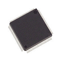
M30626FHPGP Renesas Electronics America, M30626FHPGP Datasheet - Page 35

M30626FHPGP
Manufacturer Part Number
M30626FHPGP
Description
Manufacturer
Renesas Electronics America
Datasheet
1.M30626FHPGP.pdf
(103 pages)
Specifications of M30626FHPGP
Cpu Family
M16C
Device Core Size
16/32Bit
Frequency (max)
24MHz
Interface Type
I2C/IEBus/UART
Program Memory Type
Flash
Program Memory Size
384KB
Total Internal Ram Size
31KB
# I/os (max)
87
Number Of Timers - General Purpose
11
Operating Supply Voltage (typ)
5V
Operating Supply Voltage (max)
5.5V
Operating Supply Voltage (min)
3.3V
On-chip Adc
26-chx10-bit
On-chip Dac
2-chx8-bit
Instruction Set Architecture
CISC
Operating Temp Range
-20C to 85C
Operating Temperature Classification
Commercial
Mounting
Surface Mount
Pin Count
100
Package Type
LQFP
Lead Free Status / Rohs Status
Compliant
Available stocks
Company
Part Number
Manufacturer
Quantity
Price
Company:
Part Number:
M30626FHPGP
Manufacturer:
RENESAS
Quantity:
24
Part Number:
M30626FHPGP
Manufacturer:
RENESAS/瑞萨
Quantity:
20 000
Company:
Part Number:
M30626FHPGP#U3C
Manufacturer:
Renesas
Quantity:
300
Company:
Part Number:
M30626FHPGP#U3C
Manufacturer:
Renesas
Quantity:
834
Company:
Part Number:
M30626FHPGP#U3C
Manufacturer:
Renesas Electronics America
Quantity:
10 000
Part Number:
M30626FHPGP#U5
Manufacturer:
RENESAS/瑞萨
Quantity:
20 000
Company:
Part Number:
M30626FHPGP#U5C
Manufacturer:
Renesas Electronics America
Quantity:
10 000
Part Number:
M30626FHPGP#U5C
Manufacturer:
RENESAS/瑞萨
Quantity:
20 000
Company:
Part Number:
M30626FHPGP#U7C
Manufacturer:
Renesas Electronics America
Quantity:
10 000
M16C/62P Group (M16C/62P, M16C/62PT)
Rev.2.41
REJ03B0001-0241
3.
Figure 3.1 is a Memory Map of the M16C/62P group. The address space extends the 1M bytes from address 00000h to
FFFFFh.
The internal ROM is allocated in a lower address direction beginning with address FFFFFh. For example, a 64-Kbyte
internal ROM is allocated to the addresses from F0000h to FFFFFh.
As for the flash memory version, 4-Kbyte space (block A) exists in 0F000h to 0FFFFh. 4-Kbyte space is mainly for
storing data. In addition to storing data, 4-Kbyte space also can store programs.
The fixed interrupt vector table is allocated to the addresses from FFFDCh to FFFFFh. Therefore, store the start
address of each interrupt routine here.
The internal RAM is allocated in an upper address direction beginning with address 00400h. For example, a 10-Kbyte
internal RAM is allocated to the addresses from 00400h to 02BFFh. In addition to storing data, the internal RAM also
stores the stack used when calling subroutines and when interrupts are generated.
The SRF is allocated to the addresses from 00000h to 003FFh. Peripheral function control registers are located here.
Of the SFR, any area which has no functions allocated is reserved for future use and cannot be used by users.
The special page vector table is allocated to the addresses from FFE00h to FFFDBh. This vector is used by the JMPS
or JSRS instruction. For details, refer to the M16C/60 and M16C/20 Series Software Manual.
In memory expansion and microprocessor modes, some areas are reserved for future use and cannot be used by users.
Use M16C/62P (80-pin version) and M16C/62PT in single-chip mode. The memory expansion and microprocessor
modes cannot be used
.
Figure 3.1
Memory
NOTES:
10 Kbytes
12 Kbytes
16 Kbytes
20 Kbytes
24 Kbytes
31 Kbytes
4 Kbytes
5 Kbytes
Size
1. During memory expansion and microprocessor modes, can be used.
2. In memory expansion mode, can be used.
3. As for the flash memory version, 4-Kbyte space (block A) exists.
4. Shown here is a memory map for the case where the PM10 bit in the PM1 register is “1”
5. When using the masked ROM version, write nothing to internal ROM area.
Jan 10, 2006
Internal RAM
and the PM13 bit in the PM1 register is “1”.
Address XXXXXh
013FFh
017FFh
02BFFh
033FFh
043FFh
053FFh
063FFh
07FFFh
Memory Map
128 Kbytes
192 Kbytes
256 Kbytes
320 Kbytes
384 Kbytes
512 Kbytes
48 Kbytes
64 Kbytes
96 Kbytes
Page 33 of 96
Size
Internal ROM
Address YYYYYh
F4000h
F0000h
E8000h
E0000h
D0000h
C0000h
B0000h
A0000h
80000h
(3)
XXXXXh
YYYYYh
FFFFFh
0FFFFh
00000h
00400h
0F000h
10000h
27000h
28000h
80000h
(program area)
Reserved area
Reserved area
Reserved area
External area
External area
Internal ROM
Internal ROM
(data area)
Internal RAM
SFR
(3)
(2)
(5)
(1)
FFFDCh
FFE00h
FFFFFh
Undefined instruction
BRK instruction
Watchdog timer
Address match
Special page
vector table
Single step
Overflow
Reset
DBC
NMI
3. Memory


