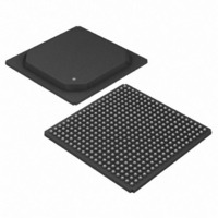
DS3172+ Maxim Integrated Products, DS3172+ Datasheet - Page 112

DS3172+
Manufacturer Part Number
DS3172+
Description
IC TXRX DS3/E3 DUAL 400-BGA
Manufacturer
Maxim Integrated Products
Datasheet
1.DS3171N.pdf
(234 pages)
Specifications of DS3172+
Function
Single-Chip Transceiver
Interface
DS3, E3
Number Of Circuits
2
Voltage - Supply
3.135 V ~ 3.465 V
Current - Supply
328mA
Operating Temperature
0°C ~ 70°C
Mounting Type
Surface Mount
Package / Case
400-BGA
Includes
DS3 Framers, E3 Framers, HDLC Controller, On-Chip BERTs
Lead Free Status / RoHS Status
Lead free / RoHS Compliant
Power (watts)
-
- Current page: 112 of 234
- Download datasheet (2Mb)
10.12.3 Detailed Description
The receiver performs clock and data recovery from an alternate mark inversion (AMI) coded signal or a B3ZS- or
HDB3-coded AMI signal and monitors for loss of the incoming signal. The transmitter drives standard pulse-shape
waveforms onto 75Ω coaxial cable. See
The jitter attenuator can be mapped into the receiver data path, mapped into the transmitter data path, or be
disabled. The DS3/E3 LIU conforms to the telecommunications standards listed in
external components required for proper operation.
Figure 10-32. DS3/E3 LIU Block Diagram
10.12.4 Transmitter
10.12.4.1 Transmit Clock
The clock used in the LIU Transmitter is typically based on either the CLAD clock or TCLKI, selected by the
CLADC bit in PORT.CR3.
10.12.4.2 Waveshaping, Line Build-Out, Line Driver
The waveshaping block converts the transmit clock, positive data, and negative data signals into a single AMI
signal with the waveshape required for interfacing to DS3/E3 lines.
(AC Timing section) show the waveform template specifications and test parameters.
Because DS3 signals must meet the waveform templates at the cross-connect through any cable length from 0 to
450ft, the waveshaping circuitry includes a selectable LBO feature. For cable lengths of 225ft or greater, the TLBO
configuration bit (PORT.CR2.TLBO) should be low. When TLBO is low, output pulses are driven onto the coaxial
cable without any preattenuation. For cable lengths less than 225ft, TLBO should be high to enable the LBO
circuitry. When TLBO is high, pulses are preattenuated by the LBO circuitry before being driven onto the coaxial
cable. The LBO circuitry provides attenuation that mimics the attenuation of 225ft of coaxial cable.
FROM DS3/E3
TO DS3/E3 LINE
LINE
TXPn
TXNn
RXPn
RXNn
VDD
VSS
Supply
Power
Analog
Local
Loopback
Monitor
Driver
CLKA
Automatic
Equalizer
Adaptive
Control
Clock Rate
Gain
Adapter
+
ALOS
CLKB
Figure 10-32
squelch
CLKC
Recovery
Clock &
Data
for a detailed functional block diagram of the DS3/E3 LIU.
112
Table 18-6
TO B3ZS/HDB3
FROM B3ZS/HDB3
through
DECODER
ENCODER
Table
Table 18-8
4-1.
Figure 1-1
and
Figure 18-9
shows the
Related parts for DS3172+
Image
Part Number
Description
Manufacturer
Datasheet
Request
R

Part Number:
Description:
MAX7528KCWPMaxim Integrated Products [CMOS Dual 8-Bit Buffered Multiplying DACs]
Manufacturer:
Maxim Integrated Products
Datasheet:

Part Number:
Description:
Single +5V, fully integrated, 1.25Gbps laser diode driver.
Manufacturer:
Maxim Integrated Products
Datasheet:

Part Number:
Description:
Single +5V, fully integrated, 155Mbps laser diode driver.
Manufacturer:
Maxim Integrated Products
Datasheet:

Part Number:
Description:
VRD11/VRD10, K8 Rev F 2/3/4-Phase PWM Controllers with Integrated Dual MOSFET Drivers
Manufacturer:
Maxim Integrated Products
Datasheet:

Part Number:
Description:
Highly Integrated Level 2 SMBus Battery Chargers
Manufacturer:
Maxim Integrated Products
Datasheet:

Part Number:
Description:
Current Monitor and Accumulator with Integrated Sense Resistor; ; Temperature Range: -40°C to +85°C
Manufacturer:
Maxim Integrated Products

Part Number:
Description:
TSSOP 14/A�/RS-485 Transceivers with Integrated 100O/120O Termination Resis
Manufacturer:
Maxim Integrated Products

Part Number:
Description:
TSSOP 14/A�/RS-485 Transceivers with Integrated 100O/120O Termination Resis
Manufacturer:
Maxim Integrated Products

Part Number:
Description:
QFN 16/A�/AC-DC and DC-DC Peak-Current-Mode Converters with Integrated Step
Manufacturer:
Maxim Integrated Products

Part Number:
Description:
TDFN/A/65V, 1A, 600KHZ, SYNCHRONOUS STEP-DOWN REGULATOR WITH INTEGRATED SWI
Manufacturer:
Maxim Integrated Products

Part Number:
Description:
Integrated Temperature Controller f
Manufacturer:
Maxim Integrated Products

Part Number:
Description:
SOT23-6/I�/45MHz to 650MHz, Integrated IF VCOs with Differential Output
Manufacturer:
Maxim Integrated Products

Part Number:
Description:
SOT23-6/I�/45MHz to 650MHz, Integrated IF VCOs with Differential Output
Manufacturer:
Maxim Integrated Products

Part Number:
Description:
EVALUATION KIT/2.4GHZ TO 2.5GHZ 802.11G/B RF TRANSCEIVER WITH INTEGRATED PA
Manufacturer:
Maxim Integrated Products

Part Number:
Description:
QFN/E/DUAL PCIE/SATA HIGH SPEED SWITCH WITH INTEGRATED BIAS RESISTOR
Manufacturer:
Maxim Integrated Products
Datasheet:


