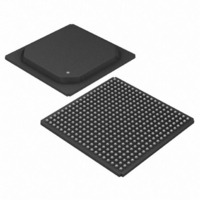
DS3172+ Maxim Integrated Products, DS3172+ Datasheet - Page 63

DS3172+
Manufacturer Part Number
DS3172+
Description
IC TXRX DS3/E3 DUAL 400-BGA
Manufacturer
Maxim Integrated Products
Datasheet
1.DS3171N.pdf
(234 pages)
Specifications of DS3172+
Function
Single-Chip Transceiver
Interface
DS3, E3
Number Of Circuits
2
Voltage - Supply
3.135 V ~ 3.465 V
Current - Supply
328mA
Operating Temperature
0°C ~ 70°C
Mounting Type
Surface Mount
Package / Case
400-BGA
Includes
DS3 Framers, E3 Framers, HDLC Controller, On-Chip BERTs
Lead Free Status / RoHS Status
Lead free / RoHS Compliant
Power (watts)
-
- Current page: 63 of 234
- Download datasheet (2Mb)
and automatic FEBE is enabled. Transmit clock comes from the CLAD CLKA pin. The pin inversion on all pins is
disabled.
Individual blocks are reset and powered down when not used determined by the settings in the line mode bits
PORT.CR2.LM[2:0] and framer mode bits PORT.CR2.FM[2:0].
10.4 Global Resources
10.4.1 Clock Rate Adapter (CLAD)
The clock rate adapter is used to create multiple clocks for LIU reference clocks or transmit clocks from a single
clock reference input on the CLKA pin. The clock frequency applied to this pin must be at the DS3 (44.736 MHz),
E3 (34.368 MHz) and STS-1 (51.84 MHz) clock rates. Given one of these clocks the other two clocks will be
generated. The internally generated signals can be driven on output pins (CLKB and CLKC) for external use.
The receive LIU is supplied a reference clock from the CLAD. The receive LIU selects the clock frequency based
upon the mode the user selects via the FM bits. The CLAD output is also available as a transmit clock source if
selected via the PORT.CR2.CLADC register bit.
The user must supply at least one of the three rates (DS3, E3, STS-1) to the CLKA pin. The CLAD[3:0] bits inform
the PLL of the frequency applied to the pins. Selection of the output clock of the CLAD applied to the LIU and
optionally the transmitter is controlled by the FM bits (located in PORT.CR2). The CLAD allows maximum flexibility
to the user. The user may supply any of the three clock rates and use the CLAD to convert the rate to the particular
clock rate needed for his application.
Figure 10-6. CLAD Block
The clock rate adapter can also be disabled and all three clocks supplied externally using the CLKA, CLKB and
CLKC pins as clock inputs. When the CLAD is disabled, the three reference clocks DS3, E3 and STS-1 will need to
be applied to the CLKA, CLKB and CLKC pins, respectively. If any of the three frequencies is not required, it does
not need to be applied to the CLAD CLK pins.
CLKC
CLKA
CLKB
CLAD MODE
CLAD
63
DS3 clock
E3 clock
CC52 clock
Related parts for DS3172+
Image
Part Number
Description
Manufacturer
Datasheet
Request
R

Part Number:
Description:
MAX7528KCWPMaxim Integrated Products [CMOS Dual 8-Bit Buffered Multiplying DACs]
Manufacturer:
Maxim Integrated Products
Datasheet:

Part Number:
Description:
Single +5V, fully integrated, 1.25Gbps laser diode driver.
Manufacturer:
Maxim Integrated Products
Datasheet:

Part Number:
Description:
Single +5V, fully integrated, 155Mbps laser diode driver.
Manufacturer:
Maxim Integrated Products
Datasheet:

Part Number:
Description:
VRD11/VRD10, K8 Rev F 2/3/4-Phase PWM Controllers with Integrated Dual MOSFET Drivers
Manufacturer:
Maxim Integrated Products
Datasheet:

Part Number:
Description:
Highly Integrated Level 2 SMBus Battery Chargers
Manufacturer:
Maxim Integrated Products
Datasheet:

Part Number:
Description:
Current Monitor and Accumulator with Integrated Sense Resistor; ; Temperature Range: -40°C to +85°C
Manufacturer:
Maxim Integrated Products

Part Number:
Description:
TSSOP 14/A�/RS-485 Transceivers with Integrated 100O/120O Termination Resis
Manufacturer:
Maxim Integrated Products

Part Number:
Description:
TSSOP 14/A�/RS-485 Transceivers with Integrated 100O/120O Termination Resis
Manufacturer:
Maxim Integrated Products

Part Number:
Description:
QFN 16/A�/AC-DC and DC-DC Peak-Current-Mode Converters with Integrated Step
Manufacturer:
Maxim Integrated Products

Part Number:
Description:
TDFN/A/65V, 1A, 600KHZ, SYNCHRONOUS STEP-DOWN REGULATOR WITH INTEGRATED SWI
Manufacturer:
Maxim Integrated Products

Part Number:
Description:
Integrated Temperature Controller f
Manufacturer:
Maxim Integrated Products

Part Number:
Description:
SOT23-6/I�/45MHz to 650MHz, Integrated IF VCOs with Differential Output
Manufacturer:
Maxim Integrated Products

Part Number:
Description:
SOT23-6/I�/45MHz to 650MHz, Integrated IF VCOs with Differential Output
Manufacturer:
Maxim Integrated Products

Part Number:
Description:
EVALUATION KIT/2.4GHZ TO 2.5GHZ 802.11G/B RF TRANSCEIVER WITH INTEGRATED PA
Manufacturer:
Maxim Integrated Products

Part Number:
Description:
QFN/E/DUAL PCIE/SATA HIGH SPEED SWITCH WITH INTEGRATED BIAS RESISTOR
Manufacturer:
Maxim Integrated Products
Datasheet:


