DS3172+ Maxim Integrated Products, DS3172+ Datasheet - Page 2
DS3172+
Manufacturer Part Number
DS3172+
Description
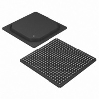
IC TXRX DS3/E3 DUAL 400-BGA
Manufacturer
Maxim Integrated Products
Datasheet
1.DS3171N.pdf
(234 pages)
Specifications of DS3172+
Function
Single-Chip Transceiver
Interface
DS3, E3
Number Of Circuits
2
Voltage - Supply
3.135 V ~ 3.465 V
Current - Supply
328mA
Operating Temperature
0°C ~ 70°C
Mounting Type
Surface Mount
Package / Case
400-BGA
Includes
DS3 Framers, E3 Framers, HDLC Controller, On-Chip BERTs
Lead Free Status / RoHS Status
Lead free / RoHS Compliant
Power (watts)
-


FEATURES (CONTINUED
DETAILED DESCRIPTION
The DS3171 (single), DS3172 (dual), DS3173 (triple), and DS3174 (quad) perform framing, formatting, and line
transmission and reception. These devices contain integrated LIU(s), framer/formatter for M23 DS3, C-bit DS3,
G.751 E3, G.832 E3, or a combination of the above signal formats.
Each LIU has independent receive and transmit paths. The receiver LIU block performs clock and data recovery
from a B3ZS- or HDB3-coded AMI signal and monitors for loss of the incoming signal, or can be bypassed for
direct clock and data inputs. The receiver LIU block optionally performs B3ZS/HDB3 decoding. The transmitter LIU
drives standard pulse-shape waveforms onto 75Ω coaxial cable or can be bypassed for direct clock and data
outputs. The jitter attenuator can be placed in either transmit or receive data path when the LIU is enabled. The
DS3/E3 framers transmit and receive serial data in properly formatted M23 DS3, C-bit DS3, G.751 E3, or G.832 E3
data streams. Unused functions can be powered down to reduce device power. The DS317x DS3/E3 SCTs
conform to the telecommunications standards listed in Section
Loopbacks Include Line, Diagnostic, Framer,
Payload, and Analog with Capabilities to Insert
AIS in the Directions Away from Loopback
Directions
Ports can be Disabled to Reduce Power
Integrated Clock Rate Adapter to Generate the
Remaining Internally Required 44.736MHz (DS3)
and 34.368MHz (E3) from a Single Clock
Reference Source at One of Three Standard
Frequencies (DS3, E3, STS-1)
)
2
4.
Pin Compatible with the DS318x Family of
Devices and the DS316x Family of Devices
8-/16-Bit Generic Microprocessor Interface
Low-Power (~1.73W) 3.3V Operation (5V
Tolerant I/O)
Small High-Density Thermally Enhanced Plastic
BGA Packaging (TE-PBGA) with 1.27mm Pitch
Industrial Temperature Operation:
-40°C to +85°C
IEEE1149.1 JTAG Test Port
Related parts for DS3172+
Image
Part Number
Description
Manufacturer
Datasheet
Request
R

Part Number:
Description:
MAX7528KCWPMaxim Integrated Products [CMOS Dual 8-Bit Buffered Multiplying DACs]
Manufacturer:
Maxim Integrated Products
Datasheet:
Part Number:
Description:
Single +5V, fully integrated, 1.25Gbps laser diode driver.
Manufacturer:
Maxim Integrated Products
Datasheet:
Part Number:
Description:
Single +5V, fully integrated, 155Mbps laser diode driver.
Manufacturer:
Maxim Integrated Products
Datasheet:
Part Number:
Description:
VRD11/VRD10, K8 Rev F 2/3/4-Phase PWM Controllers with Integrated Dual MOSFET Drivers
Manufacturer:
Maxim Integrated Products
Datasheet:
Part Number:
Description:
Highly Integrated Level 2 SMBus Battery Chargers
Manufacturer:
Maxim Integrated Products
Datasheet:
Part Number:
Description:
Current Monitor and Accumulator with Integrated Sense Resistor; ; Temperature Range: -40°C to +85°C
Manufacturer:
Maxim Integrated Products
Part Number:
Description:
TSSOP 14/A�/RS-485 Transceivers with Integrated 100O/120O Termination Resis
Manufacturer:
Maxim Integrated Products
Part Number:
Description:
TSSOP 14/A�/RS-485 Transceivers with Integrated 100O/120O Termination Resis
Manufacturer:
Maxim Integrated Products
Part Number:
Description:
QFN 16/A�/AC-DC and DC-DC Peak-Current-Mode Converters with Integrated Step
Manufacturer:
Maxim Integrated Products
Part Number:
Description:
TDFN/A/65V, 1A, 600KHZ, SYNCHRONOUS STEP-DOWN REGULATOR WITH INTEGRATED SWI
Manufacturer:
Maxim Integrated Products
Part Number:
Description:
Integrated Temperature Controller f
Manufacturer:
Maxim Integrated Products
Part Number:
Description:
SOT23-6/I�/45MHz to 650MHz, Integrated IF VCOs with Differential Output
Manufacturer:
Maxim Integrated Products
Part Number:
Description:
SOT23-6/I�/45MHz to 650MHz, Integrated IF VCOs with Differential Output
Manufacturer:
Maxim Integrated Products
Part Number:
Description:
EVALUATION KIT/2.4GHZ TO 2.5GHZ 802.11G/B RF TRANSCEIVER WITH INTEGRATED PA
Manufacturer:
Maxim Integrated Products
Part Number:
Description:
QFN/E/DUAL PCIE/SATA HIGH SPEED SWITCH WITH INTEGRATED BIAS RESISTOR
Manufacturer:
Maxim Integrated Products
Datasheet: