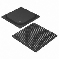
DS3172+ Maxim Integrated Products, DS3172+ Datasheet - Page 74

DS3172+
Manufacturer Part Number
DS3172+
Description
IC TXRX DS3/E3 DUAL 400-BGA
Manufacturer
Maxim Integrated Products
Datasheet
1.DS3171N.pdf
(234 pages)
Specifications of DS3172+
Function
Single-Chip Transceiver
Interface
DS3, E3
Number Of Circuits
2
Voltage - Supply
3.135 V ~ 3.465 V
Current - Supply
328mA
Operating Temperature
0°C ~ 70°C
Mounting Type
Surface Mount
Package / Case
400-BGA
Includes
DS3 Framers, E3 Framers, HDLC Controller, On-Chip BERTs
Lead Free Status / RoHS Status
Lead free / RoHS Compliant
Power (watts)
-
- Current page: 74 of 234
- Download datasheet (2Mb)
Table 10-19
Table 10-19. Payload (Downstream) AIS Enable Modes
10.5.4 Loop Timing Mode
Loop timing mode is enabled by setting the PORT.CR3.LOOPT bit. This mode replaces the clock from the TCLKIn
pin with the internal receive clock from either the RLCLKn pin if the RX LIU is disabled, or the recovered clock from
the RX LIU if it is enabled. The loop-timing mode can be activated in any framing or line interface mode.
10.5.5 HDLC Overhead Controller
The data signal to the receive HDLC controller will be forced to a one while still being clocked when the framer
(DS3, E3), to which the HDLC is connected, detects LOF or AIS. Forcing the data signal to all ones will cause an
HDLC packet abort if the data started to look like a packet instead of allowing a bad, and possibly very long, HDLC
packet.
10.5.6 Trail Trace
There is a single Trail Trace controller for use in line maintenance protocols. The E3-G.832 framer has access to
the trail trace controller.
10.5.7 BERT
There is a Bit Error Rate Test (BERT) circuit for each port for use in generating and detecting test signals in the
payload bits. The BERT can generate and detect PRBS patterns up to 2^32-1 bits as well as repeating patterns up
to 32 bits long. The generated BERT signal replaces the data on the TSERn pin in SCT modes when the BERT is
enabled by setting the PORT.CR1.BENA.
When the BERT is enabled The TDENn and RDENn pins will still be active but the data on the TSERn pin will be
discarded.
10.5.8 SCT port pins
The SCT port pins have multiple functions based on the framing mode the device is in as well as other pin mode
select bits.
10.5.8.1 Transmit SCT port pins
The transmit SCT pins are TSOFIn, TSERn, TSOFOn / TDENn, and TCLKOn / TGCLKn. They have different
functions based on the framing mode and other pin mode bits. Unused input pin functions should drive a logic zero
into the device circuits expecting a signal from that pin. The control bits that configure the pins’ modes are
PORT.CR2.FM[2:0], PORT.CR3.TPFPE, PORT.CR3.TSOFOS and PORT.CR3.TCLKS.
PORT.CR1
PAIS[2:0]
000
001
010
011
100
101
110
111
lists the PAIS decodes for various payload AIS enable modes.
When AIS is sent
Always
When LLB (no DLB) active
When PLB active
When LLB(no DLB) or PLB active
When LOS (no DLB) active
When OOF active
When OOF, LOS. LLB (no DLB), or
PLB active
Never
AIS Code
74
none
UA1
UA1
UA1
UA1
UA1
UA1
UA1
Related parts for DS3172+
Image
Part Number
Description
Manufacturer
Datasheet
Request
R

Part Number:
Description:
MAX7528KCWPMaxim Integrated Products [CMOS Dual 8-Bit Buffered Multiplying DACs]
Manufacturer:
Maxim Integrated Products
Datasheet:

Part Number:
Description:
Single +5V, fully integrated, 1.25Gbps laser diode driver.
Manufacturer:
Maxim Integrated Products
Datasheet:

Part Number:
Description:
Single +5V, fully integrated, 155Mbps laser diode driver.
Manufacturer:
Maxim Integrated Products
Datasheet:

Part Number:
Description:
VRD11/VRD10, K8 Rev F 2/3/4-Phase PWM Controllers with Integrated Dual MOSFET Drivers
Manufacturer:
Maxim Integrated Products
Datasheet:

Part Number:
Description:
Highly Integrated Level 2 SMBus Battery Chargers
Manufacturer:
Maxim Integrated Products
Datasheet:

Part Number:
Description:
Current Monitor and Accumulator with Integrated Sense Resistor; ; Temperature Range: -40°C to +85°C
Manufacturer:
Maxim Integrated Products

Part Number:
Description:
TSSOP 14/A�/RS-485 Transceivers with Integrated 100O/120O Termination Resis
Manufacturer:
Maxim Integrated Products

Part Number:
Description:
TSSOP 14/A�/RS-485 Transceivers with Integrated 100O/120O Termination Resis
Manufacturer:
Maxim Integrated Products

Part Number:
Description:
QFN 16/A�/AC-DC and DC-DC Peak-Current-Mode Converters with Integrated Step
Manufacturer:
Maxim Integrated Products

Part Number:
Description:
TDFN/A/65V, 1A, 600KHZ, SYNCHRONOUS STEP-DOWN REGULATOR WITH INTEGRATED SWI
Manufacturer:
Maxim Integrated Products

Part Number:
Description:
Integrated Temperature Controller f
Manufacturer:
Maxim Integrated Products

Part Number:
Description:
SOT23-6/I�/45MHz to 650MHz, Integrated IF VCOs with Differential Output
Manufacturer:
Maxim Integrated Products

Part Number:
Description:
SOT23-6/I�/45MHz to 650MHz, Integrated IF VCOs with Differential Output
Manufacturer:
Maxim Integrated Products

Part Number:
Description:
EVALUATION KIT/2.4GHZ TO 2.5GHZ 802.11G/B RF TRANSCEIVER WITH INTEGRATED PA
Manufacturer:
Maxim Integrated Products

Part Number:
Description:
QFN/E/DUAL PCIE/SATA HIGH SPEED SWITCH WITH INTEGRATED BIAS RESISTOR
Manufacturer:
Maxim Integrated Products
Datasheet:


