DS3172+ Maxim Integrated Products, DS3172+ Datasheet - Page 50

DS3172+
Manufacturer Part Number
DS3172+
Description
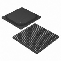
IC TXRX DS3/E3 DUAL 400-BGA
Manufacturer
Maxim Integrated Products
Datasheet
1.DS3171N.pdf
(234 pages)
Specifications of DS3172+
Function
Single-Chip Transceiver
Interface
DS3, E3
Number Of Circuits
2
Voltage - Supply
3.135 V ~ 3.465 V
Current - Supply
328mA
Operating Temperature
0°C ~ 70°C
Mounting Type
Surface Mount
Package / Case
400-BGA
Includes
DS3 Framers, E3 Framers, HDLC Controller, On-Chip BERTs
Lead Free Status / RoHS Status
Lead free / RoHS Compliant
Power (watts)
-
- Current page: 50 of 234
- Download datasheet (2Mb)
10 FUNCTIONAL DESCRIPTION
10.1 Processor Bus Interface
10.1.1 8/16 Bit Bus Widths
The external processor bus can be sized for 8 or 16 bits using the WIDTH pin. When in 8-bit mode (WIDTH=0), the
address is composed of all the address bits including A[0], the lower 8 data lines D[7:0] are used and the upper 8
data lines D[15:8] are not used and never driven during a read cycle. When in 16-bit mode (WIDTH=1), the
address bus does not include A[0] (the LSB of the address bus is not routed to the chip) and all 16 data lines
D[15:0] are used. See
10.1.2 Ready Signal (RDY)
The RDY signal allows the microprocessor to use the minimum bus cycle period for maximum efficiency. When this
signal goes low, the RD or WR cycle can be terminated. See
NOTE: The RDY signal will not go active if the user attempts to read or write unused ports or unused registers not
assigned to any design blocks. The RDY signal will go active if the user writes or reads reserved registers or
unused registers within design blocks.
10.1.3 Byte Swap Modes
The processor interface can operate in byte swap mode when the data bus is configured for 16-bit operation. The
A[0]/BSWAP pin is used to determine whether byte swapping is enabled. This pin should be static and not change
while operating. When the A[0]/BSWAP pin is low the upper register bits REG[15:8] are mapped to the upper
external data bus lines D[15:8], and the lower register bits REG[7:0] are mapped to the lower external data bus
lines D[7:0]. When the A[0]/BSWAP pin is high the upper register bits REG[15:8] are mapped to the lower external
data bus lines D[7:0], and the lower register bits REG[7:0] are mapped to the upper external data bus lines D[15:8].
See
10.1.4 Read-Write / Data Strobe Modes
The processor interface can operate in either read-write strobe mode or data strobe mode. When MODE=0 the
read-write strobe mode is enabled and a negative pulse on RD performs a read cycle, and a negative pulse on WR
performs a write cycle. When MODE=1 the data strobe mode is enabled and a negative pulse on DS when R/W is
high performs a read cycle, and a negative pulse on DS when R/W is low performs a write cycle. The read-write
strobe mode is commonly called the “Intel” mode, and the data strobe mode is commonly called the “Motorola”
mode.
10.1.5 Clear on Read / Clear on Write Modes
The latched status register bits can be programmed to clear on a read access or clear on a write access. The
global control register bit GL.CR1.LSBCRE controls the mode that all of the latched registers are cleared. When
LSBCRE=0, the latched register bits will be cleared when the register is written to and the write data has the
register bits to clear set. When LSBCRE=1, the latched register bits that are set will be cleared when the register is
read.
The clear on write mode expects the user to use the following protocol:
This protocol is useful when multiple uncoordinated software tasks access the same latched register. Each task
should only clear the bits with which it is concerned; the other tasks will clear the bits with which they are
concerned.
Figure 8-23
and
Figure 8-24
Figure 8-19
1. Read the latched status register
2. Write to the registers with the bits set that need to be cleared.
for functional timing diagrams.
and
Figure 8-21
for functional timing diagrams.
50
Figure 8-27
for functional timing diagrams.
Related parts for DS3172+
Image
Part Number
Description
Manufacturer
Datasheet
Request
R

Part Number:
Description:
MAX7528KCWPMaxim Integrated Products [CMOS Dual 8-Bit Buffered Multiplying DACs]
Manufacturer:
Maxim Integrated Products
Datasheet:

Part Number:
Description:
Single +5V, fully integrated, 1.25Gbps laser diode driver.
Manufacturer:
Maxim Integrated Products
Datasheet:

Part Number:
Description:
Single +5V, fully integrated, 155Mbps laser diode driver.
Manufacturer:
Maxim Integrated Products
Datasheet:

Part Number:
Description:
VRD11/VRD10, K8 Rev F 2/3/4-Phase PWM Controllers with Integrated Dual MOSFET Drivers
Manufacturer:
Maxim Integrated Products
Datasheet:

Part Number:
Description:
Highly Integrated Level 2 SMBus Battery Chargers
Manufacturer:
Maxim Integrated Products
Datasheet:

Part Number:
Description:
Current Monitor and Accumulator with Integrated Sense Resistor; ; Temperature Range: -40°C to +85°C
Manufacturer:
Maxim Integrated Products

Part Number:
Description:
TSSOP 14/A�/RS-485 Transceivers with Integrated 100O/120O Termination Resis
Manufacturer:
Maxim Integrated Products

Part Number:
Description:
TSSOP 14/A�/RS-485 Transceivers with Integrated 100O/120O Termination Resis
Manufacturer:
Maxim Integrated Products

Part Number:
Description:
QFN 16/A�/AC-DC and DC-DC Peak-Current-Mode Converters with Integrated Step
Manufacturer:
Maxim Integrated Products

Part Number:
Description:
TDFN/A/65V, 1A, 600KHZ, SYNCHRONOUS STEP-DOWN REGULATOR WITH INTEGRATED SWI
Manufacturer:
Maxim Integrated Products

Part Number:
Description:
Integrated Temperature Controller f
Manufacturer:
Maxim Integrated Products

Part Number:
Description:
SOT23-6/I�/45MHz to 650MHz, Integrated IF VCOs with Differential Output
Manufacturer:
Maxim Integrated Products

Part Number:
Description:
SOT23-6/I�/45MHz to 650MHz, Integrated IF VCOs with Differential Output
Manufacturer:
Maxim Integrated Products

Part Number:
Description:
EVALUATION KIT/2.4GHZ TO 2.5GHZ 802.11G/B RF TRANSCEIVER WITH INTEGRATED PA
Manufacturer:
Maxim Integrated Products

Part Number:
Description:
QFN/E/DUAL PCIE/SATA HIGH SPEED SWITCH WITH INTEGRATED BIAS RESISTOR
Manufacturer:
Maxim Integrated Products
Datasheet:


