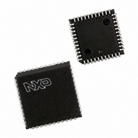
SC26C92C1A,518 NXP Semiconductors, SC26C92C1A,518 Datasheet - Page 13

SC26C92C1A,518
Manufacturer Part Number
SC26C92C1A,518
Description
IC DUART SOT187-2
Manufacturer
NXP Semiconductors
Datasheet
1.SC26C92C1A518.pdf
(31 pages)
Specifications of SC26C92C1A,518
Number Of Channels
2, DUART
Package / Case
44-LCC (J-Lead)
Features
Transceiver
Fifo's
8 Byte
Voltage - Supply
5V
With Auto Flow Control
Yes
With False Start Bit Detection
Yes
With Modem Control
Yes
With Cmos
Yes
Mounting Type
Surface Mount
Data Rate
0.2304 MBd
Supply Voltage (max)
5.5 V
Supply Voltage (min)
4.5 V
Supply Current
10 mA
Maximum Operating Temperature
+ 70 C
Minimum Operating Temperature
0 C
Mounting Style
SMD/SMT
Operating Supply Voltage
5 V
Lead Free Status / RoHS Status
Lead free / RoHS Compliant
Lead Free Status / RoHS Status
Lead free / RoHS Compliant, Lead free / RoHS Compliant
Other names
568-5047-2
935051510518
SC26C92C1A,518
SC26C92C1A-T
SC26C92C1A-T
935051510518
SC26C92C1A,518
SC26C92C1A-T
SC26C92C1A-T
Philips Semiconductors
Mode, command, clock select, and status registers are duplicated
for each channel to provide total independent operation and control.
Refer to Table 2 for register bit descriptions.
Table 1. SC26C92 Register Addressing
NOTE:
The three MR Registers are accessed via the MR Pointer and Commands 1xh and Bxh. (Where “x” represents receiver and transmitter enable/
disable control)
Table 2. Register Bit Formats
NOTE: *In block error mode, block error conditions must be cleared by using the error reset command (command 4x) or a receiver reset.
2000 Jan 31
The following named registers are the same for Channels
A and B
Mode Register
Status Register
Clock Select
Command Register
Receiver FIFO
Transmitter FIFO
Returns F on read
Dual universal asynchronous receiver/transmitter (DUART)
A3
MR0B[3:0] are
MR0A, MR0B
0
0
0
0
0
0
0
0
1
1
1
1
1
1
1
1
MR1A
MR1B
MR1B
0x00
reserved
d
A2
0
0
0
0
1
1
1
1
0
0
0
0
1
1
1
1
Rx CONTROLS
0 = No
1 = Yes
BIT 7
RTS
Rx WATCH
0 = Disable
1 = Enable
A1
0
0
1
1
0
0
1
1
0
0
1
1
0
0
1
1
RxFIFOA
BIT 7
TxFIFOA
DOG
MRnA
CSRA
SRA
CRA
A0
0 = RxRDY
1 = FFULL
0
1
0
1
0
1
0
1
0
1
0
1
0
1
0
1
Rx INT
BIT 6
BIT 1
MR0 description
RxFIFOB
TxFIFOB
See Tables in
MRnB
CSRB
RxINT BIT 2
SRB
CRB
The reserved
BIT 6
Mode Register A (MR0A, MR1A, MR2A)
Status Register A (SRA)
Reserved
Rx Holding Register A (RxFIFOA)
Input Port Change Register (IPCR)
Interrupt Status Register (ISR)
Counter/Timer Upper Value (CTU)
Counter/Timer Lower Value (CTL)
Mode Register B (MR0B, MR1B, MR2B)
Status Register B (SRB)
Reserved
Rx Holding Register B (RxFIFOB)
User Defined Flag/Status Flag
Input Ports IP0 to IP6
Start Counter Command
Stop Counter Command
ERROR
0 = Char
1 = Block
MODE
W only
W only
W only
BIT 5
R only
R only
R/W
READ (RDN = 0)
BIT 5 BIT 4
TxINT (1:0)
13
BIT 4
00 = With Parity
01 = Force Parity
10 = No Parity
11 = Multidrop Mode
PARITY MODE
registers at addresses H‘02’ and H‘0A’ should never be read during
normal operation since they are reserved for internal diagnostics.
These registers control the functions which service both
Channels
Input Port Change Register
Auxiliary Control Register
Interrupt Status Register
Interrupt Mask Register
Counter Timer Upper Value
Counter Timer Lower Value
Counter Timer Preset Upper
Counter Timer Preset Lower
Input Port Register
Output Configuration Register
Set Output Port Bits
Reset Output Port Bits
Returns 1 on read
Set to 0
DON’T
CARE
BIT 3
BIT 3
Mode Register A (MR0A, MR1A, MR2A)
Clock Select Register A (CSRA)
Command Register A (CRA)
Tx Holding Register A (TxFIFOA)
Aux. Control Register (ACR)
Interrupt Mask Register (IMR)
C/T Upper Preset Value (CTPU)
C/T Lower Preset Value (CTPL)
Mode Register B (MR0B, MR1B, MR2B)
Clock Select Register B (CSRB)
Command Register B (CRB)
Tx Holding Register B (TxFIFOB)
User Defined Flag/Status Flag
Output Port Conf. Register (OPCR)
Set Output Port Bits Command (SOP12)
Reset Output Port Bits Command (ROP12)
EXTENDED II
BAUD RATE
1 = Extend II
0 = Even
PARITY
1 = Odd
0 = Normal
TYPE
BIT 2
BIT 2
WRITE (WRN = 0)
TEST 2
Set to 0
BIT 1
BIT 1
OPCR
SOPR
ROPR
CTPU
CTPL
IPCR
ACR
CTU
CTL
IMR
ISR
IPR
CHARACTER
Product specification
BITS PER
SC26C92
00 = 5
01 = 6
10 = 7
11 = 8
EXTENDED 1
BAUD RATE
0 = Normal
1 = Extend
BIT 0
BIT 0
W
W
W
W
W
W
W
R
R
R
R
R


