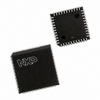
SC26C92C1A,518 NXP Semiconductors, SC26C92C1A,518 Datasheet - Page 7

SC26C92C1A,518
Manufacturer Part Number
SC26C92C1A,518
Description
IC DUART SOT187-2
Manufacturer
NXP Semiconductors
Datasheet
1.SC26C92C1A518.pdf
(31 pages)
Specifications of SC26C92C1A,518
Number Of Channels
2, DUART
Package / Case
44-LCC (J-Lead)
Features
Transceiver
Fifo's
8 Byte
Voltage - Supply
5V
With Auto Flow Control
Yes
With False Start Bit Detection
Yes
With Modem Control
Yes
With Cmos
Yes
Mounting Type
Surface Mount
Data Rate
0.2304 MBd
Supply Voltage (max)
5.5 V
Supply Voltage (min)
4.5 V
Supply Current
10 mA
Maximum Operating Temperature
+ 70 C
Minimum Operating Temperature
0 C
Mounting Style
SMD/SMT
Operating Supply Voltage
5 V
Lead Free Status / RoHS Status
Lead free / RoHS Compliant
Lead Free Status / RoHS Status
Lead free / RoHS Compliant, Lead free / RoHS Compliant
Other names
568-5047-2
935051510518
SC26C92C1A,518
SC26C92C1A-T
SC26C92C1A-T
935051510518
SC26C92C1A,518
SC26C92C1A-T
SC26C92C1A-T
1. Parameters are valid over specified temperature range.
2. All voltage measurements are referenced to ground (GND). For testing, all inputs swing between 0.4V and 3.0V with a transition time of 5ns
3. Typical values are at +25 C, typical supply voltages, and typical processing parameters.
4. Test conditions for outputs: C
5. Timing is illustrated and referenced to the WRN and RDN inputs. Also, CEN may be the ‘strobing’ input. CEN and RDN (also CEN and
6. If CEN is used as the ‘strobing’ input, the parameter defines the minimum High times between one CEN and the next. The RDN signal must
7. Minimum frequencies are not tested but are guaranteed by design. Crystal frequencies 2 to 4 MHz.
8. Clocks for 1X mode should be symmetrical.
Philips Semiconductors
AC CHARACTERISTICS
V
NOTES:
2000 Jan 31
CC
SYMBOL
t
t
t
t
t
t
t
t
t
t
t
t
t
t
t
t
f
t
f
t
f
t
f
t
t
t
t
RES
AS
AH
CS
CH
RW
DD
DF
DS
DH
RWD
PS
PH
PD
IR
CLK
CLK
CTC
CTC
RX
RX
TX
TX
TXD
TCS
RXS
RXH
Dual universal asynchronous receiver/transmitter (DUART)
Reset Timing (See Figure 3)
Bus Timing
Port Timing
Interrupt Timing (See Figure 6)
Clock Timing (See Figure 7)
Transmitter Timing (See Figure 8)
Receiver Timing (See Figure 9)
maximum. For X1/CLK this swing is between 0.4V and 4.4V. All time measurements are referenced at input voltages of 0.8V and 2.0V and
output voltages of 0.8V and 2.0V, as appropriate.
WRN) are ORed internally. The signal asserted last initiates the cycle and the signal negated first terminates the cycle.
be negated for t
= 5V
10%, T
5
5
RESET pulse width
A0-A3 setup time to RDN, WRN Low
A0-A3 hold time from RDN, WRN Low
CEN setup time to RDN, WRN Low
CEN hold time from RDN, WRN High
WRN, RDN pulse width
Data valid after RDN Low
Data bus floating after RDN High
Data setup time before WRN or CEN High
Data hold time after WRN or CEN High
High time between reads and/or writes
Port input setup time before RDN Low
Port input hold time after RDN High
OP
INTRN (or OP3-OP7 when used as interrupts) negated from:
X1/CLK High or Low time
X1/CLK frequency
CTCLK (IP2) High or Low time
CTCLK (IP2) frequency
RxC High or Low time (16X)
RxC frequency (16X)
TxC High or Low time (16X)
TxC frequency (16X)
TxD output delay from TxC external clock input on IP pin
Output delay from TxC low at OP pin to TxD data output
RxD data setup time before RxC high at external clock input on IP pin
RxD data hold time after RxC high at external clock input on IP pin
(See Figure 4)
(See Figure 5)
n
Read RxFIFO (RxRDY/FFULL interrupt)
Write TxFIFO (TxRDY interrupt)
Reset command (break change interrupt)
Stop C/T command (counter interrupt)
Read IPCR (input port change interrupt)
Write IMR (clear of interrupt mask bit)
A
RWD
output valid from WRN High
= –40 C to 85 C, unless otherwise specified.
to guarantee that any status register changes are valid.
1, 2, 4
(1X)
(1X)
L
= 150pF, except interrupt outputs. Test conditions for interrupt outputs: C
8
8
PARAMETER
5, 6
7
Min
200
0.1
10
25
70
25
30
50
55
30
30
50
50
0
0
0
0
0
0
0
0
0
0
L
= 50pF, R
LIMITS
3.6864
Typ
5
3
L
= 2.7K to V
Product specification
Max
100
100
100
100
100
100
100
SC26C92
55
25
16
16
60
30
8
8
1
1
CC
UNIT
MHz
MHz
MHz
MHz
MHz
MHz
ns
ns
ns
ns
ns
ns
ns
ns
ns
ns
ns
ns
ns
ns
ns
ns
ns
ns
ns
ns
ns
ns
ns
ns
ns
ns
ns
ns
.


