LM49200TLX/NOPB National Semiconductor, LM49200TLX/NOPB Datasheet - Page 20
LM49200TLX/NOPB
Manufacturer Part Number
LM49200TLX/NOPB
Description
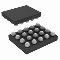
IC AUDIO SUB 1.25W AB 20USMD
Manufacturer
National Semiconductor
Series
Boomer®r
Type
Class ABr
Datasheet
1.LM49200TLNOPB.pdf
(26 pages)
Specifications of LM49200TLX/NOPB
Output Type
2-Channel (Stereo) with Stereo Headphones
Max Output Power X Channels @ Load
1.25W x 2 @ 8 Ohm; 38mW x 2 @ 32 Ohm
Voltage - Supply
2.7 V ~ 5.5 V
Features
Depop, Differential Inputs, I²C, Shutdown, Thermal Protection, Volume Control
Mounting Type
Surface Mount
Package / Case
20-MicroSMD
Lead Free Status / RoHS Status
Lead free / RoHS Compliant
Other names
LM49200TLX


www.national.com
of the application can be reduced from the free air value, re-
sulting in higher P
to any of the leads connected to the LM49200. It is especially
effective when connected to V
Refer to the application information on the LM49200 refer-
ence design board for an example of good heat sinking. If
T
made. These changes can include reduced supply voltage,
higher load impedance, or reduced ambient temperature. In-
ternal power dissipation is a function of output power. Refer
to the Typical Performance Characteristics curves for
power dissipation information for different output powers and
output loading.
POWER SUPPLY BYPASSING
As with any amplifier, proper supply bypassing is critical for
low noise performance and high power supply rejection. The
capacitor location on both the bypass and power supply pins
should be as close to the device as possible. Typical appli-
cations employ a 5V regulator with 10µF tantalum or elec-
trolytic capacitor and a ceramic bypass capacitor which aid in
supply stability. This does not eliminate the need for bypass-
ing the supply nodes of the LM49200. The selection of a
bypass capacitor, especially C
requirements, click and pop performance, system cost, and
size constraints.
GROUND REFERENCED HEADPHONE AMPLIFIER
The LM49200 features a low noise inverting charge pump that
generates an internal negative supply voltage. This allows the
headphone outputs to be biased about GND instead of a
nominal DC voltage, like traditional headphone amplifiers.
Because there is no DC component, the large DC blocking
capacitors (typically 220μF) are not necessary. The coupling
capacitors are replaced by two small ceramic charge pump
capacitors, saving board space and cost. Eliminating the out-
put coupling capacitors also improves low frequency re-
sponse. In traditional headphone amplifiers, the headphone
impedance and the output capacitor from a high-pass filter
that not only blocks the DC component of the output, but also
attenuates low frequencies, impacting the bass response.
Because the LM49200 does not require the output coupling
capacitors, the low frequency response of the device is not
degraded by external components. In addition to eliminating
the output coupling capacitors, the ground referenced output
nearly doubles the available dynamic range of the LM49200
JMAX
still exceeds 150°C, then additional changes must be
DMAX
. Additional copper foil can be added
DD
B
, is dependent upon PSRR
, GND, and the output pins.
20
headphone amplifiers when compared to a traditional head-
phone amplifier operating from the same supply voltage.
INPUT CAPACITOR SELECTION
Input capacitors may be required for some applications, or
when the audio source is single-ended. Input capacitors block
the DC component of the audio signal, eliminating any conflict
between the DC component of the audio source and the bias
voltage of the LM49200. The input capacitors create a high-
pass filter with the input resistors R
high-pass filter is found using equation below.
Where the value of R
tics Table.
High-pass filtering the audio signal helps protect the speak-
ers. When the LM49200 is using a single-ended source,
power supply noise on the ground is seen as an input signal.
Setting the high-pass filter point above the power supply noise
frequencies, 217Hz in a GSM phone, for example, filters out
the noise such that it is not amplified and heard on the output.
Capacitors with a tolerance of 10% or better are recommend-
ed for impedance matching and improved CMRR and PSRR.
CHARGE PUMP FLYING CAPACITOR (C
The flying capacitor (C1), see Figure 1, affects the load reg-
ulation and output impedance of the charge pump. A C1 value
that is too low results in a loss of current drive, leading to a
loss of amplifier headroom. A higher valued C1 improves load
regulation and lowers charge pump output impedance to an
extent. Above 2.2μF, the R
and the ESR of C1 and Cs5 dominate the output impedance.
A lower value capacitor can be used in systems with low max-
imum output power requirements.
CHARGE PUMP HOLD CAPACITOR (C
The value and ESR of the hold capacitor (Cs5) directly affects
the ripple on CPV
output ripple. Decreasing the ESR of Cs5 reduces both output
ripple and charge pump output impedance. A lower value ca-
pacitor can be used in systems with low maximum output
power requirements.
f = 1 / 2
SS
. Increasing the value of Cs5 reduces
IN
π
is given in the Electrical Characteris-
R
DS(ON)
IN
C
IN
of the charge pump switches
(Hz)
IN
. The -3dB point of the
S3
1
)
)
(2)
Related parts for LM49200TLX/NOPB
Image
Part Number
Description
Manufacturer
Datasheet
Request
R

Part Number:
Description:
IC AUDIO SUBSYSTEM AB 20-USMD
Manufacturer:
National Semiconductor
Datasheet:

Part Number:
Description:
National Semiconductor [8-Bit D/A Converter]
Manufacturer:
National Semiconductor
Datasheet:
Part Number:
Description:
National Semiconductor [Media Coprocessor]
Manufacturer:
National Semiconductor
Datasheet:
Part Number:
Description:
Digitally Controlled Tone and Volume Circuit with Stereo Audio Power Amplifier, Microphone Preamp Stage and National 3D Sound
Manufacturer:
National Semiconductor
Datasheet:
Part Number:
Description:
Digitally Controlled Tone and Volume Circuit with Stereo Audio Power Amplifier, Microphone Preamp Stage and National 3D Sound
Manufacturer:
National Semiconductor
Datasheet:
Part Number:
Description:
AC97 Rev 2 Codec with Sample Rate Conversion and National 3D Sound
Manufacturer:
National Semiconductor
Part Number:
Description:
Manufacturer:
National Semiconductor
Datasheet:
Part Number:
Description:
Manufacturer:
National Semiconductor
Datasheet:
Part Number:
Description:
General Purpose, Low Voltage, Low Power, Rail-to-Rail Output Operational Amplifiers
Manufacturer:
National Semiconductor
Datasheet:
Part Number:
Description:
8-bit 20 MSPS flash A/D converter.
Manufacturer:
National Semiconductor
Datasheet:
Part Number:
Description:
Low Noise Quad Operational Amplifier
Manufacturer:
National Semiconductor
Datasheet:
Part Number:
Description:
Quad Differential Line Receivers
Manufacturer:
National Semiconductor
Datasheet:
Part Number:
Description:
Quad High Speed Trapezoidal? Bus Transceiver
Manufacturer:
National Semiconductor
Datasheet:
Part Number:
Description:
Dual Line Receiver
Manufacturer:
National Semiconductor
Datasheet: