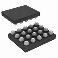
LM49200TLX/NOPB National Semiconductor, LM49200TLX/NOPB Datasheet - Page 5

LM49200TLX/NOPB
Manufacturer Part Number
LM49200TLX/NOPB
Description
IC AUDIO SUB 1.25W AB 20USMD
Manufacturer
National Semiconductor
Series
Boomer®r
Type
Class ABr
Datasheet
1.LM49200TLNOPB.pdf
(26 pages)
Specifications of LM49200TLX/NOPB
Output Type
2-Channel (Stereo) with Stereo Headphones
Max Output Power X Channels @ Load
1.25W x 2 @ 8 Ohm; 38mW x 2 @ 32 Ohm
Voltage - Supply
2.7 V ~ 5.5 V
Features
Depop, Differential Inputs, I²C, Shutdown, Thermal Protection, Volume Control
Mounting Type
Surface Mount
Package / Case
20-MicroSMD
Lead Free Status / RoHS Status
Lead free / RoHS Compliant
Other names
LM49200TLX
I
I
V
P
THD+N
SNR
DD
SD
Symbol
OS
O
Absolute Maximum Ratings
If Military/Aerospace specified devices are required,
please contact the National Semiconductor Sales Office/
Distributors for availability and specifications.
Electrical Characteristics V
The following specifications apply for V
LS = Loudspeaker, HP = Headphone.
Supply Voltage (Note 1)
Storage Temperature
Voltage at Any Input Pin
Power Dissipation (Note 3)
ESD Rating (Note 4)
ESD Rating (Note 5)
Junction Temperature (T
Soldering Information
Vapor Phase (60sec.)
Quiescent Power Supply Current
Shutdown Current
Output Offset Voltage
Output Power
Total Harmonic Distortion + Noise
Signal-to-Noise Ratio
Parameter
JMAX
)
GND − 0.3 to V
DD
= 3.3V, T
−65°C to +150°C
Internally Limited
V
EP Receiver
(Output Mode Bit D4 = 1)
Stereo LS only (Mode 2)
Stereo HP only (Mode 8)
Stereo LS + Stereo HP (Mode 10)
V
LS output, R
HP output, R
LS output, Mode 2, R
THD+N = 1%, f = 1kHz
HP output, Mode 8, R
THD+N = 1%, f = 1kHz
LS output, f = 1kHz, R
P
HP output, f = 1kHz, R
P
LS output, f = 1kHz,
V
Gain = 0dB, A-weighted
LIN & RIN AC terminated
HP output, f = 1kHz,
V
Gain = 0dB, A-weighted
LIN & RIN AC terminated
DD
IN
IN
O
O
REF
REF
(Notes 1, 2)
= 250mW, Mode 2
= 12mW, Mode 8
= 0, No Loads
= 0V, Mode 10
DD
= 3.3V
= V
= V
A
2000V
+ 0.3V
150°C
215°C
= 25°C, all volume controls set to 0dB, unless otherwise specified.
200V
OUT
OUT
6.0V
L
L
(1%THD+N)
(1%THD+N)
= 8Ω BTL
= 32Ω SE
Conditions
(Notes 1, 2)
5
L
L
L
Operating Ratings
L
= 8Ω BTL
See AN-1112 “Micro SMD Wafer Level Chip Scale
Package”
Thermal Resistance
θ
Temperature Range
Supply Voltage (V
Supply Voltage (I
= 32Ω SE
= 8Ω BTL
= 32Ω SE
T
Infrared (15sec.)
JA
MIN
≤
T
A
≤
T
MAX
2
DD
CV
)
DD
(Note 6)
Typical
)
0.02
0.05
0.02
520
105
101
1.2
4.5
7.0
2.5
1.4
38
4
LM49200
(Note 7)
Limits
450
1.7
5.5
6.4
9.8
1.7V
15
35
1
5
−40°C
2.7V
≤
I
I
≤
2
2
≤
CV
CV
V
www.national.com
T
45.1°C/W
DD
mA (max)
mA (max)
mA (max)
mA (max)
mV (max)
mV (max)
mW (min)
mW (min)
µA (max)
DD
A
DD
(Limits)
Units
≤
≤
≤
220°C
dB
dB
≤
%
%
85°C
5.5V
5.5V
V
DD


