BLF6G15L-40RN NXP Semiconductors, BLF6G15L-40RN Datasheet
BLF6G15L-40RN


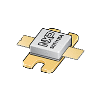
Related parts for BLF6G15L-40RN


BLF6G15L-40RN Summary of contents
Page 1
... BLF6G15L-40RN; BLF6G15LS-40RN Power LDMOS transistor Rev. 1 — 27 October 2011 1. Product profile 1.1 General description 40 W LDMOS power transistor for base station applications at frequencies from 1450 MHz to 1550 MHz. Table 1. Typical RF performance at T Test signal 2-carrier W-CDMA [1] Test signal: 3GPP test model 1; 64 DPCH; PAR = 7 probability of 0. CCDF carrier; ...
Page 2
... NXP Semiconductors 2. Pinning information Table 2. Pin BLF6G15L-40RN (SOT1135A BLF6G15LS-40RN (SOT1135B [1] Connected to flange. 3. Ordering information Table 3. Type number BLF6G15L-40RN BLF6G15LS-40RN 4. Limiting values Table 4. In accordance with the Absolute Maximum Rating System (IEC 60134). Symbol stg T j BLF6G15L-40RN_6G15LS-40RN ...
Page 3
... Symbol P L(AV D ACPR BLF6G15L-40RN_6G15LS-40RN Objective data sheet Thermal characteristics thermal resistance from junction to case T Characteristics C per section; unless otherwise specified drain-source breakdown voltage gate-source threshold voltage drain leakage current drain cut-off current gate leakage current forward transconductance ...
Page 4
... Note 1. millimeter dimensions are derived from the original inch dimensions. 2. dimension is measured 0.030 inch (0.76 mm) from the body. Outline version IEC SOT1135A Fig 1. Package outline SOT1135A BLF6G15L-40RN_6G15LS-40RN Objective data sheet ...
Page 5
... Note 1. millimeter dimensions are derived from the original inch dimensions. 2. dimension is measured 0.030 inch (0.76 mm) from the body. Outline version IEC SOT1135B Fig 2. Package outline SOT1135B BLF6G15L-40RN_6G15LS-40RN Objective data sheet ...
Page 6
... CW LDMOS PAR DPCH RF VSWR W-CDMA 11. Revision history Table 9. Revision history Document ID BLF6G15L-40RN_6G15LS-40RN v.1 BLF6G15L-40RN_6G15LS-40RN Objective data sheet Abbreviations Description 3rd Generation Partnership Project Complementary Cumulative Distribution Function Continuous Wave Laterally Diffused Metal-Oxide Semiconductor Peak-to-Average power Ratio Dedicated Physical Channel Radio Frequency ...
Page 7
... Suitability for use — NXP Semiconductors products are not designed, authorized or warranted to be suitable for use in life support, life-critical or safety-critical systems or equipment, nor in applications where failure or BLF6G15L-40RN_6G15LS-40RN Objective data sheet [3] Definition This document contains data from the objective specification for product development. ...
Page 8
... Contact information For more information, please visit: For sales office addresses, please send an email to: BLF6G15L-40RN_6G15LS-40RN Objective data sheet NXP Semiconductors’ specifications such use shall be solely at customer’s own risk, and (c) customer fully indemnifies NXP Semiconductors for any liability, damages or failed product claims resulting from customer design and use of the product for automotive applications beyond NXP Semiconductors’ ...
Page 9
... Please be aware that important notices concerning this document and the product(s) described herein, have been included in section ‘Legal information’. © NXP B.V. 2011. For more information, please visit: http://www.nxp.com For sales office addresses, please send an email to: salesaddresses@nxp.com Document identifier: BLF6G15L-40RN_6G15LS-40RN All rights reserved. Date of release: 27 October 2011 ...