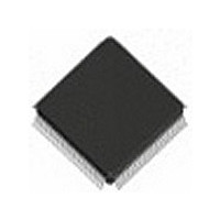
IDT72V3674L15PF IDT, Integrated Device Technology Inc, IDT72V3674L15PF Datasheet - Page 31

IDT72V3674L15PF
Manufacturer Part Number
IDT72V3674L15PF
Description
IC FIFO 16384X36 15NS 128QFP
Manufacturer
IDT, Integrated Device Technology Inc
Series
72Vr
Datasheet
1.IDT72V3654L15PF8.pdf
(37 pages)
Specifications of IDT72V3674L15PF
Function
Asynchronous
Memory Size
576K (16K x 36)
Data Rate
67MHz
Access Time
15ns
Voltage - Supply
3.15 V ~ 3.45 V
Operating Temperature
0°C ~ 70°C
Mounting Type
Surface Mount
Package / Case
128-TQFP, 128-VQFP
Configuration
Dual
Density
576Kb
Access Time (max)
10ns
Word Size
36b
Organization
8Kx36x2
Sync/async
Synchronous
Expandable
No
Bus Direction
Bi-Directional
Package Type
TQFP
Clock Freq (max)
66.7MHz
Operating Supply Voltage (typ)
3.3V
Operating Supply Voltage (min)
3.15V
Operating Supply Voltage (max)
3.45V
Supply Current
400mA
Operating Temp Range
0C to 70C
Operating Temperature Classification
Commercial
Mounting
Surface Mount
Pin Count
128
Lead Free Status / RoHS Status
Contains lead / RoHS non-compliant
Other names
72V3674L15PF
NOTES:
1. t
2. FIFO1 Write (CSA = LOW, W/RA = LOW, MBA = LOW), FIFO1 read (CSB = LOW, W/RB = HIGH, MBB = LOW). Data in the FIFO1 output register has been read from the FIFO.
3. If Port B size is word or byte, AEB is set LOW by the last word or byte read from FIFO1, respectively.
NOTES:
1. t
2. FIFO2 Write (CSB = LOW, W/RB = LOW, MBB = LOW), FIFO2 read (CSA = LOW, W/RA = LOW, MBA = LOW). Data in the FIFO2 output register has been read from the FIFO.
3. If Port B size is word or byte, t
NOTES:
1. t
2. FIFO1 Write (CSA = LOW, W/RA = HIGH, MBA = LOW), FIFO1 read (CSB = LOW, W/RB = HIGH, MBB = LOW). Data in the FIFO1 output register has been read from the FIFO.
3. D = Maximum FIFO Depth = 2,048 for the IDT72V3654, 4,096 for the IDT72V3664, 8,192 for the IDT72V3674.
4. If Port B size is word or byte, t
CLKA
CLKB
CLKB
CLKA
CLKA
CLKB
IDT72V3654/72V3664/72V3674 3.3V CMOS SyncBiFIFO
2,048 x 36 x 2, 4,096 x 36 x 2 and 8,192 x 36 x 2
ENA
ENB
AEA
AEB
ENB
ENA
ENA
CLKB edge is less than t
CLKA edge is less than t
AFA
ENB
CLKB edge is less than t
SKEW2
SKEW2
SKEW2
is the minimum time between a rising CLKA edge and a rising CLKB edge for AEB to transition HIGH in the next CLKB cycle. If the time between the rising CLKA edge and rising
is the minimum time between a rising CLKB edge and a rising CLKA edge for AEA to transition HIGH in the next CLKA cycle. If the time between the rising CLKB edge and rising
is the minimum time between a rising CLKA edge and a rising CLKB edge for AFA to transition HIGH in the next CLKA cycle. If the time between the rising CLKA edge and rising
X1 Words in FIFO1
X2 Words in FIFO2
[D-(Y1+1)] Words in FIFO1
t
t
ENS2
ENS2
SKEW2
SKEW2
SKEW2
t
ENS2
Figure 23. Timing for AEB
Figure 24. Timing for AEA
SKEW2
SKEW2
, then AEB may transition HIGH one CLKB cycle later than shown.
, then AEA may transition HIGH one CLKA cycle later than shown.
, then AFA may transition HIGH one CLKA cycle later than shown.
Figure 25. Timing for AFA
is referenced to the rising CLKB edge that writes the last word or byte of the long word, respectively.
is referenced to the rising CLKB edge that reads the last word or byte of the long word, respectively.
t
t
t
ENH
SKEW2
ENH
t
SKEW2
t
t
ENH
PAF
(1)
(1)
AEB
AEB
AEB
AEB when FIFO1 is Almost-Empty (IDT Standard and FWFT Modes)
AEA
AEA
AEA
AEA when FIFO2 is Almost-Empty (IDT Standard and FWFT Modes)
AFA
AFA
AFA
AFA when FIFO1 is Almost-Full (IDT Standard and FWFT Modes)
1
1
t
ENS2
TM
WITH BUS-MATCHING
31
t
SKEW2
t
(D-Y1) Words in FIFO1
ENH
2
2
t
(1)
PAE
t
PAE
1
COMMERCIAL TEMPERATURE RANGE
(X2+1) Words in FIFO2
(X1+1) Words in FIFO1
t
t
ENS2
ENS2
2
t
PAF
t
t
ENH
ENH
t
t
PAE
PAE
4664 drw 27
4664 drw 26
4664 drw 25


