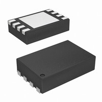
ISL9206DRZ-T Intersil, ISL9206DRZ-T Datasheet - Page 13

ISL9206DRZ-T
Manufacturer Part Number
ISL9206DRZ-T
Description
IC AUTHENTICATION BATTERY 8-TDFN
Manufacturer
Intersil
Series
FlexiHash+™r
Datasheet
1.ISL9206DHZ-T.pdf
(17 pages)
Specifications of ISL9206DRZ-T
Function
Battery Authentication
Battery Type
Li-Ion, Li-Pol, NiMH
Voltage - Supply
2.6 V ~ 4.8 V
Operating Temperature
-20°C ~ 85°C
Mounting Type
Surface Mount
Package / Case
8-TDFN Exposed Pad
Lead Free Status / RoHS Status
Lead free / RoHS Compliant
Available stocks
Company
Part Number
Manufacturer
Quantity
Price
Company:
Part Number:
ISL9206DRZ-T
Manufacturer:
SEMTECH
Quantity:
300
ADDRESS
ADDRESS
RW Read/Write
WC Clear after write Zeros read
RC Clear after read
<> Default setting loaded from designated OTP ROM bit
W Write-only
W Writing disabled after lock-out
R
BIT
7:6
5:4
1:0
BIT
6:4
3:0
3
2
7
1-00
1-01
2-00
2-01
2-05
Read-only
locations
TYPE
TABLE 13. LEGEND FOR THE TYPE COLUMN
TOSC[3:0]
DAB[1:0]
SPD[1:0]
SLO[1:0]
TIBB[2:0]
NAME
NAME
ASLP
eINT
HSF
NAME
MSCR
NAME
CHLG
AUTH
SESL
STAT
Data read
Zeros read
Data read
Data read, then
cleared
TYPE
TYPE
READ ACTION
RW
RW
RW
RW
RW
R
R
R
Authentication Code Register
Challenge Code Register
13
Secrets Selection
TABLE 11. DEFAULT CONFIGURATION (DCFG) REGISTER SETTINGS
DESCRIPTION
DESCRIPTION
Master Control
Device Status
DEFAULT
DEFAULT
TABLE 12. DEFAULT TRIMMING (DTRM) REGISTER SETTINGS
00
01
00
1
1
--
--
0
TABLE 9. CONTROL AND STATUS REGISTERS (BANK 1)
TABLE 10. AUTHENTICATION REGISTERS (BANK 2)
Data ignored
Data written
Data written
Data ignored
Data written, then
cleard
WRITE ACTION
Device Address Bit Setting:
00 : device responds only when CS field in instruction frame is’0’
01 : device responds to any CS field value in instruction frame
10 : device responds to any CS field value in instruction frame
11 : device responds only when CS field in instruction frame is ‘1’
XSD Bus Speed Setting: Configures the bit rate of the XSD bus interface.
00 : 0.5x (2.89kbps)
01 : 1x (5.78kbps)
10 : 2x (11.56kbps)
11 : 4x (23.12kbps)
Power-on default setting of eINT bit in the MSCR register.
Power-on default setting of ASLP bit in the MSCR register.
Secrets Lock-out Bits:
Bit 1 : Read/Write lock-out bit for address locations 0-02 to 0-09 (Secret Set #1 & #2)
Bit 0 : Read/Write lock-out bit for address locations 0-0A to 0-0D (Secret Set #3)
NOTE: Once Bit 0 or Bit 1 is set, writing to the OTP ROM will permanently be disabled
(after a reset cycle).
Unused
Reference Current Trim Setting
Oscillator Frequency Trim Setting
eEEW
sEEW
BIT 7
BIT 7
--
ISL9206
sBER
BIT 6
BIT 6
eINT
--
ADDRESS 0-00: DEFAULT CONFIGURATION (DCFG)
This address location stores the default configuration when
the ISL9206 is manufactured. Table 11 describes each bit in
detail. The legend for the TYPE column is given in Table 13.
ADDRESS 0-01: DEFAULT TRIM SETTING (DTRM)
This address location is writable only when the device is in
test mode. During normal operation, any data written to it will
be ignored. Table 12 describes the DTRM address in detail.
ADDRESS 0-02/03/04/05: AUTHENTICATION SECRET
SET #1 (SE1A/B/C/D)
These address locations store the first set of secrets to be
used for hash calculation. Reading and writing to this
register can be disabled by setting the SLO[1] bit at OTP
ROM location 0-00[1].
sACC
BIT 5
BIT 5
--
--
DESCRIPTION
DESCRIPTION
BIT 4
BIT 4
--
--
--
CHLG[31:0]
AUTH[7:0]
BIT3
BIT3
--
DAB[1:0]
CSL[1:0]
BIT 2
BIT 2
--
ASLP
BIT 1
BIT 1
SLO[1:0]
SSL[1:0]
January 5, 2007
SRST
BIT 0
BIT 0
FN9260.2


