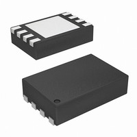
ISL9206DRZ-T Intersil, ISL9206DRZ-T Datasheet - Page 2

ISL9206DRZ-T
Manufacturer Part Number
ISL9206DRZ-T
Description
IC AUTHENTICATION BATTERY 8-TDFN
Manufacturer
Intersil
Series
FlexiHash+™r
Datasheet
1.ISL9206DHZ-T.pdf
(17 pages)
Specifications of ISL9206DRZ-T
Function
Battery Authentication
Battery Type
Li-Ion, Li-Pol, NiMH
Voltage - Supply
2.6 V ~ 4.8 V
Operating Temperature
-20°C ~ 85°C
Mounting Type
Surface Mount
Package / Case
8-TDFN Exposed Pad
Lead Free Status / RoHS Status
Lead free / RoHS Compliant
Available stocks
Company
Part Number
Manufacturer
Quantity
Price
Company:
Part Number:
ISL9206DRZ-T
Manufacturer:
SEMTECH
Quantity:
300
Electrical Specifications
Absolute Maximum Ratings
Supply Voltage (VDD) . . . . . . . . . . . . . . . . . . . . . . . . . . . . . . . . 5.5V
All Other Pins . . . . . . . . . . . . . . . . . . . . . . . . . . . . . -0.5 to V
ESD Rating
Recommended Operating Conditions
Ambient Temperature Range . . . . . . . . . . . . . . . . . . .-20°C to +85°C
CAUTION: Stresses above those listed in “Absolute Maximum Ratings” may cause permanent damage to the device. This is a stress only rating and operation of the
device at these or any other conditions above those indicated in the operational sections of this specification is not implied.
NOTE:
DC CHARACTERISTICS
Supply Voltage
Run Mode Supply Current
(exclude I/O current)
Sleep Mode Supply Current:
OTP Programming Mode Supply Current
Internal Regulated Supply Voltage
Internal OTP ROM Programming Voltage
POR Release Threshold
POR Assertion Threshold
XSD PIN CHARACTERISTICS
XSD Input Low Voltage
XSD Input High Voltage
XSD Input Hysteresis
XSD Internal Pull-Down Current
XSD Output Low Voltage
XSD Input Transition Time
XSD Output Fall Time
XSD Pin Capacitance
XSD BUS TIMING CHARACTERISTICS (Refer to XSD Bus Symbol Timing Definitions Tables)
Programming Bit Rate
XSD Input Deglitch Time
1. θ
2. θ
3. For θ
Human Body Model (Per MIL-STD-883 Method 3015.7) . . .4000V
Machine Model (Per EIAJ ED-4701 Method C-111) . . . . . . . .400V
CDM . . . . . . . . . . . . . . . . . . . . . . . . . . . . . . . . . . . . . . . . . .1000V
Tech Brief TB379.
JA
JA
is measured with the component mounted on a high effective thermal conductivity test board in free air. See Tech Brief TB379 for details.
is measured in free air with the component mounted on a high effective thermal conductivity test board with “direct attach” features. See
JC
, the “case temp” location is the center of the exposed metal pad on the package underside.
PARAMETER
2
Unless otherwise noted, all parameters are guaranteed over the operational supply voltage and temperature
range of the device as follows: T
(Reference to GND)
SYMBOL
V
V
T
V
I
I
C
V
V
V
POR+
V
I
DDS
DDP
POR-
V
I
WDG
V
HYS
DD
PD
t
t
PIN
DD
RG
PP
OL
IH
X
F
IL
During normal operation
During OTP ROM programming
V
V
V
For ~ 1.8ms duration per write operation
Observable only in test mode
Observable only in test mode
V
V
V
I
10% to 90% transition time
90% to 10%, C
x = 0.5 to 4
Pulse width narrower than the deglitch time will not cause
the device to wake up
OL
DD
DD
DD
DD
DD
DD
= 1mA
= 4.2V
= 4.8V
= 4.2V, XSD pin floating
= 2.6V
= 4.2V
= 4.8V
DD
+0.5V
ISL9206
A
LOAD
= -20°C to +85°C; V
TEST CONDITIONS
= 12pF
Thermal Information
Thermal Resistance (Typical)
Maximum Junction Temperature (Plastic Package) . . . . . . . +125°C
Maximum Storage Temperature Range . . . . . . . . . .-40°C to +125°C
Maximum Lead Temperature (Soldering 10s) . . . . . . . . . . . . +300°C
SOT-23 Package (Note 1) . . . . . . . . . .
2x3 TDFN Package (Notes 2, 3) . . . . .
DD
= 2.6V to 4.8V.
2.89
MIN
-0.4
2.6
2.8
2.3
1.9
1.5
1.5
11
7
-
-
-
-
-
-
-
-
-
-
-
-
θ
JA
TYP
0.15
110
120
250
400
2.5
2.2
1.8
0.8
1.2
1.8
12
6
-
-
-
-
-
-
-
-
-
200
(°C/W)
70
V
23.12
MAX
0.4V
140
160
500
4.8
4.8
0.5
2.7
2.4
2.1
0.5
2.0
2.5
0.4
DD
13
50
20
2
-
-
-
January 5, 2007
θ
+
JC
10.5
N/A
FN9260.2
(°C/W)
UNITS
kHz
mV
μA
μA
μA
μA
μA
μA
μA
pF
μs
ns
μs
V
V
V
V
V
V
V
V
V


