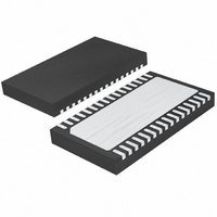
LTC4268IDKD-1#TRPBF Linear Technology, LTC4268IDKD-1#TRPBF Datasheet - Page 10

LTC4268IDKD-1#TRPBF
Manufacturer Part Number
LTC4268IDKD-1#TRPBF
Description
IC PD HIGH POWER W/CNTRL 32-DFN
Manufacturer
Linear Technology
Type
Power over Ethernet Switch (PoE)r
Datasheet
1.LTC4268CDKD-1PBF.pdf
(48 pages)
Specifications of LTC4268IDKD-1#TRPBF
Applications
Remote Peripherals (Industrial Controls, Cameras, Data Access)
Internal Switch(s)
Yes
Operating Temperature
-40°C ~ 85°C
Mounting Type
Surface Mount
Package / Case
32-WFDFN Exposed Pad
Lead Free Status / RoHS Status
Lead free / RoHS Compliant
Available stocks
Company
Part Number
Manufacturer
Quantity
Price
PIN FUNCTIONS
LTC4268-1
SFST (Pin 14): Soft-Start. This pin, in conjunction with a
capacitor (C
primary current through the sense resistor. It is also used
to control converter inrush at start-up. The SFST clamps
the V
start is complete. The ramp time is approximately 70ms
per μF of capacitance. Leave SFST open if not using the
soft-start function.
OSC (Pin 15): Oscillator. This pin in conjunction with an
external capacitor (C
oscillator frequency. The frequency is approximately
100kHz • 100/C
FB (Pin 16): Feedback Amplifi er Input. Feedback is usually
sensed via a third winding and enabled during the fl yback
period. This pin also sinks additional current to compensate
for load current variation as set by the R
Thevenin equivalent resistance of the feedback divider at
roughly 3k.
V
used for frequency compensation of the switcher control
loop. It is the output of the feedback amplifi er and the input
to the current comparator. Switcher frequency compensa-
tion components are normally placed on this pin to GND.
The voltage on this pin is proportional to the peak primary
switch current. The feedback amplifi er output is enabled
during the synchronous switch on time.
UVLO (Pin 18): Undervoltage Lockout. A resistive divider
from V
upon V
threshold, the gate drives are disabled, but the part draws its
normal quiescent current from V
lockout supersedes this function so V
10
CMP
CMP
(Pin 17): Frequency Compensation Control. V
IN
IN
to this pin sets an undervoltage lockout based
level (not V
voltage and thus limits peak current until soft-
SFST
OSC
) to GND, controls the ramp-up of peak
(pF).
CC
OSC
). When the UVLO pin is below its
) to GND defi nes the controller
CC
. The V
CC
CMP
CC
must be great
undervoltage
pin. Keep the
CMP
is
enough to start the part. The bias current on this pin has
hysteresis such that the bias current is sourced when UVLO
threshold is exceeded. This introduces a hysteresis at the
pin equivalent to the bias current change times the imped-
ance of the upper divider resistor. The user can control
the amount of hysteresis by adjusting the impedance of
the divider. Tie the UVLO pin to V
this function. See the Applications Information for details.
This pin is used for the UVLO function of the switching
regulator. The PD interface section has an UVLO defi ned
by the IEEE 802.3af specifi cation.
SENSE–, SENSE+ (Pins 19, 20): Current Sense Inputs.
These pins are used to measure primary side switch cur-
rent through an external sense resistor. Peak primary side
current is used in the converter control loop. Make Kelvin
connections to the sense resistor R
problems. SENSE– connects to the GND side. At maximum
current (V
100mV threshold. The signal is blanked (ignored) during
the minimum turn-on time.
C
Connect a capacitor from C
the effects of parasitic resistances in the feedback sens-
ing path. A 0.1μF ceramic capacitor suffi ces for most
applications. Short this pin to GND in less demanding
applications.
R
Connect a resistor from R
pensate for parasitic resistances in the feedback sensing
path. In less demanding applications, this resistor is not
needed and this pin can be left open. See Applications
Information for details.
CMP
CMP
(Pin 21): Load Compensation Capacitive Control.
(Pin 22): Load Compensation Resistive Control.
CMP
at its maximum voltage) SENSE pins have
CMP
CMP
to GND in order to reduce
to GND in order to com-
CC
SENSE
if you are not using
to reduce noise
42681fb


