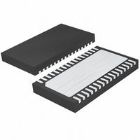
LTC4268IDKD-1#TRPBF Linear Technology, LTC4268IDKD-1#TRPBF Datasheet - Page 38

LTC4268IDKD-1#TRPBF
Manufacturer Part Number
LTC4268IDKD-1#TRPBF
Description
IC PD HIGH POWER W/CNTRL 32-DFN
Manufacturer
Linear Technology
Type
Power over Ethernet Switch (PoE)r
Datasheet
1.LTC4268CDKD-1PBF.pdf
(48 pages)
Specifications of LTC4268IDKD-1#TRPBF
Applications
Remote Peripherals (Industrial Controls, Cameras, Data Access)
Internal Switch(s)
Yes
Operating Temperature
-40°C ~ 85°C
Mounting Type
Surface Mount
Package / Case
32-WFDFN Exposed Pad
Lead Free Status / RoHS Status
Lead free / RoHS Compliant
Available stocks
Company
Part Number
Manufacturer
Quantity
Price
APPLICATIONS INFORMATION
LTC4268-1
In operation, the “trickle charge” resistor R
to V
of 1mA to charge C
draws only its start-up current. When C
turn-on threshold voltage the LTC4268-1 turns on abruptly
and draws its normal supply current.
Switching action commences and the converter begins to
deliver power to the output. Initially the output voltage is
low and the fl yback voltage is also low, so C
most of the LTC4268-1 current (only a fraction comes
from R
time, typically tens of milliseconds, the output voltage
approaches its desired value. The fl yback winding then
provides the LTC4268-1 supply current and the V
stabilizes.
If C
before stabilization and the LTC4268-1 turns off. The V
node then begins to charge back up via R
threshold, where the part again turns on. Depending upon
the circuit, this may result in either several on-off cycles
before proper operation is reached, or permanent relaxation
oscillation at the V
R
current greater than the maximum rated LTC4268-1 start-up
current, and a worst-case maximum charging current less
than the minimum rated LTC4268-1 supply current.
38
TR
R
R
and
TR
IN
is selected to yield a worst-case minimum charging
TR(MAX)
TR(MIN)
is undersized, V
and supplies a small current, typically on the order
TR
.) V
Figure 16. V
>
CC
<
V
V
voltage continues to drop until after some
IN(MAX)
IN(MIN)
V
CC
CMP
17
TR
I
CC
CC(ST _ MAX)
node.
CMP
. Initially the LTC4268-1 is off and
I
CC(MIN)
− V
− V
reaches the V
Compensation Network
42681 F16
CC(ON _ MAX)
CC(ON _ MIN)
C
VCMP2
R
VCMP
C
VCMP
CC
TR
turn-off threshold
TR
reaches the V
TR
to the turn-on
is connected
TR
CC
supplies
voltage
CC
CC
Make C
behavior described above. This is complicated to deter-
mine theoretically as it depends on the particulars of the
secondary circuit and load behavior. Empirical testing is
recommended. Note that the use of the optional soft-start
function lengthens the power-up timing and requires a
correspondingly larger value for C
The LTC4268-1 has an internal clamp on V
mately 20V. This provides some protection for the part
in the event that the switcher is off (UVLO low) and the
V
should never attain this clamp voltage.
Control Loop Compensation
Loop frequency compensation is performed by connect-
ing a capacitor network from the output of the feedback
amplifi er (V
Because of the sampling behavior of the feedback amplifi er,
compensation is different from traditional current mode
controllers. Normally only C
be used to add a “zero” but the phase margin improvement
traditionally offered by this extra resistor is usually already
accomplished by the nonzero secondary circuit impedance.
C
pole and is usually sized at 0.1 times C
In further contrast to traditional current mode switchers,
V
The dynamic nature of the clamped feedback amplifi er
forms an effective track/hold type response, whereby the
V
“held” during the subsequent “switch on” portion of the
next cycle. This action naturally holds the V
stable during the current comparator sense action (current
mode switching).
Application Note 19 provides a method for empirically
tweaking frequency compensation. Basically it involves
introducing a load current step and monitoring the
response.
CC
VCMP2
CMP
CMP
node is pulled high. If R
pin ripple is generally not an issue with the LTC4268-1.
voltage changes during the fl yback pulse, but is then
TR
can be used to add an additional high frequency
large enough to avoid the relaxation oscillatory
CMP
pin) to ground as shown in Figure 16.
VCMP
TR
is sized correctly the part
is required. R
TR
.
VCMP
CC
.
CMP
of approxi-
VCMP
voltage
42681fb
can


