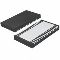
LTC4268IDKD-1#TRPBF Linear Technology, LTC4268IDKD-1#TRPBF Datasheet - Page 35

LTC4268IDKD-1#TRPBF
Manufacturer Part Number
LTC4268IDKD-1#TRPBF
Description
IC PD HIGH POWER W/CNTRL 32-DFN
Manufacturer
Linear Technology
Type
Power over Ethernet Switch (PoE)r
Datasheet
1.LTC4268CDKD-1PBF.pdf
(48 pages)
Specifications of LTC4268IDKD-1#TRPBF
Applications
Remote Peripherals (Industrial Controls, Cameras, Data Access)
Internal Switch(s)
Yes
Operating Temperature
-40°C ~ 85°C
Mounting Type
Surface Mount
Package / Case
32-WFDFN Exposed Pad
Lead Free Status / RoHS Status
Lead free / RoHS Compliant
Available stocks
Company
Part Number
Manufacturer
Quantity
Price
APPLICATIONS INFORMATION
assume that our worst-case conditions yield an I
above nominal so I
on R
110% = 88mV/2.3A and nominal R
to the nearest available lower value, 33mΩ.
Selecting the Load Compensation Resistor
The expression for R
section as:
Continuing the example:
This value for R
methods are required for producing the best results. This is
because several of the required input variables are diffi cult
to estimate precisely. For instance, the ESR term above
includes that of the transformer secondary, but its effective
ESR value depends on high frequency behavior, not simply
DC winding resistance. Similarly, K1 appears as a simple
ratio of V
estimating effi ciency is not a simple calculation.
The suggested empirical method is as follows:
1. Build a prototype of the desired supply including the
actual secondary components.
R
If ESR + R
CMP
SENSE
K1=
DC=
R
CMP
= K1•
⎛
⎝ ⎜
1+
IN
and minimum V
V
= 0.116 •
= 3.25k
V
IN
N•V
to V
DS(ON)
OUT
• Eff
R
CMP
V
1
ESR + R
IN(NOM)
SENSE
OUT
OUT
PK
⎞
⎠ ⎟
is a good starting point, but empirical
= 8mΩ
=
33mΩ • 1− 0.455
CMP
= 2.3A. If there is a 10% tolerance
times effi ciency, but theoretically
48 • 90%
• 1− DC
(
=
DS(ON)
was derived in the Operation
1+
5
SENSE
8mΩ
(
8
1
1
)
•
= 0.116
• R1• N
= 88mV, then R
48
SENSE
5
= 45.5%
)
SF
= 35mΩ. Round
• 37.4kΩ •
PK
SENSE
of 40%
3
1
•
2. Temporarily ground the C
3. Calculate a value for the K1 constant based on V
4. Compute:
5. Verify this result by connecting a resistor of this value
6. Disconnect the ground short to C
compensation function. Measure output voltage while
sweeping output current over the expected range.
Approximate the voltage variation as a straight line.
ΔV
and the measured effi ciency.
from the R
fi lter capacitor to ground. Measure the output imped-
ance R
in place. R
Fine tuning is accomplished experimentally by slightly
altering R
where R′
resistor. R
in place and R
load compensation (from step 2).
R
′ R
CMP
CMP
OUT
/ΔI
= K1•
S(OUT)
= R
C MP
Figure 14. f
OUT
300
200
100
CMP
S(OUT)CMP
CMP
50
S(OUT)
CMP
is the new value for the load compensation
R
R
= ΔV
= R
. A revised estimate for R
S(OUT)
SENSE
S(OUT)
• 1+
pin to ground.
30
⎛
⎜
⎝
S(OUT)
OUT
should have decreased signifi cantly.
OSC
is the output impedance with R
R
/ΔI
is the output impedance with no
• R1• N
vs OSC Capacitor Values
S(OUT)CMP
R
.
OUT
S(OUT)
C
OSC
CMP
with the new compensation
(pF)
SF
100
pin to disable the load
CMP
LTC4268-1
⎞
⎟
⎠
and connect a 0.1μF
42681 F14
CMP
200
is:
IN
35
, V
42681fb
CMP
OUT


