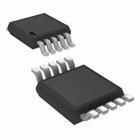
LM25061PMM-2/NOPB National Semiconductor, LM25061PMM-2/NOPB Datasheet - Page 10

LM25061PMM-2/NOPB
Manufacturer Part Number
LM25061PMM-2/NOPB
Description
IC CTLR POS HOTSWAP AUTO 10MSOP
Manufacturer
National Semiconductor
Type
Hot-Swap Controllerr
Datasheet
1.LM25061PMME-2NOPB.pdf
(20 pages)
Specifications of LM25061PMM-2/NOPB
Applications
General Purpose
Internal Switch(s)
No
Voltage - Supply
2.9 V ~ 17 V
Operating Temperature
-40°C ~ 85°C
Mounting Type
Surface Mount
Package / Case
10-TFSOP, 10-MSOP (0.118", 3.00mm Width)
Lead Free Status / RoHS Status
Lead free / RoHS Compliant
Other names
LM25061PMM-2
Available stocks
Company
Part Number
Manufacturer
Quantity
Price
Company:
Part Number:
LM25061PMM-2/NOPB
Manufacturer:
NS
Quantity:
12 112
www.national.com
control the current delivered to the load. During the in-rush
limiting interval (t2 in
current source charges C
input current reduce below their respective limiting thresholds
before the TIMER pin reaches 1.72V the 80 µA current source
is switched off, and C
current sink (t3 in
Gate Control
A charge pump provides the voltage at the GATE pin to en-
hance the N-Channel MOSFET’s gate. During normal oper-
ating conditions (t3 in Figure 3) the gate of Q1 is held charged
by an internal 20 µA current source. The voltage at the GATE
pin (with respect to ground) is limited by an internal 19.5V
zener diode. See the graph “GATE Pin voltage”. Since the
gate-to-source voltage applied to Q1 could be as high as
19.5V during various conditions, a zener diode with the ap-
propriate voltage rating must be added between the GATE
and OUT pins if the maximum V
MOSFET is less than 19.5V. The external zener diode must
have a forward current rating of at least 260 mA.
When the system voltage is initially applied, the GATE pin is
held low by a 260 mA pull-down current. This helps prevent
an inadvertent turn-on of the MOSFET through its drain-gate
capacitance as the applied system voltage increases.
Figure
Figure
T
is discharged by the internal 2.5 µA
T
. If Q1’s power dissipation and the
3). The in-rush limiting interval is
3) an internal 80 µA fault timer
GS
FIGURE 3. Power Up Sequence (Current Limit only)
rating of the selected
10
complete when the load current reduces to the normal oper-
ating level. The PGD pin switches high when the output
voltage exceeds the threshold programmed at the FB pin.
If the TIMER pin voltage reaches 1.72V before in-rush current
limiting or power limiting ceases (during t2), a fault is declared
and Q1 is turned off. See the Fault Timer & Restart section
for a complete description of the fault mode.
During the insertion time (t1 in
low by a 2 mA pull-down current. This maintains Q1 in the off-
state until the end of t1, regardless of the voltage at VIN or
UVLO.
Following the insertion time, during t2 in
voltage of Q1 is modulated to keep the current or power dis-
sipation level from exceeding the programmed levels. While
in the current or power limiting mode the TIMER pin capacitor
is charging. If the current and power limiting cease before the
TIMER pin reaches 1.72V the TIMER pin capacitor then dis-
charges, and the circuit enters normal operation.
If the in-rush limiting condition persists such that the TIMER
pin reached 1.72V during t2, the GATE pin is then pulled low
by the 2 mA pull-down current. The GATE pin is then held low
until either a power up sequence is initiated (LM25061-1), or
until the end of the restart sequence (LM25061-2). See the
Fault Timer & Restart section.
Figure
3) the GATE pin is held
Figure
30090313
3, the gate


