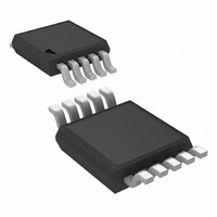
LM25061PMM-2/NOPB National Semiconductor, LM25061PMM-2/NOPB Datasheet - Page 13

LM25061PMM-2/NOPB
Manufacturer Part Number
LM25061PMM-2/NOPB
Description
IC CTLR POS HOTSWAP AUTO 10MSOP
Manufacturer
National Semiconductor
Type
Hot-Swap Controllerr
Datasheet
1.LM25061PMME-2NOPB.pdf
(20 pages)
Specifications of LM25061PMM-2/NOPB
Applications
General Purpose
Internal Switch(s)
No
Voltage - Supply
2.9 V ~ 17 V
Operating Temperature
-40°C ~ 85°C
Mounting Type
Surface Mount
Package / Case
10-TFSOP, 10-MSOP (0.118", 3.00mm Width)
Lead Free Status / RoHS Status
Lead free / RoHS Compliant
Other names
LM25061PMM-2
Available stocks
Company
Part Number
Manufacturer
Quantity
Price
Company:
Part Number:
LM25061PMM-2/NOPB
Manufacturer:
NS
Quantity:
12 112
basing it on the current limit value provides a more reliable
design since the circuit can operate near the current limit
threshold continuously. The resistor’s surge capability must
also be considered since the circuit breaker threshold is ap-
proximately twice the current limit threshold. Connections
from R
POWER LIMIT THRESHOLD
The LM25061 determines the power dissipation in the exter-
nal MOSFET (Q1) by monitoring the drain current (the current
in R
at the PWR pin (R
for Q1, and is calculated from the following equation:
where P
and R
Limit section. For example, if R
power limit threshold is 20W, R
Q1’s power dissipation reaches the threshold Q1’s gate is
modulated to regulate the load current, keeping Q1’s power
from exceeding the threshold. For proper operation of the
power limiting feature, R
power limiting circuit is active, the fault timer is active as de-
scribed in the Fault Timer & Restart section. Typically, power
limit is reached during startup, or if the output voltage falls due
to a severe overload or short circuit.
The programmed maximum power dissipation should have a
reasonable margin from the maximum power defined by the
FET's SOA chart if the LM25061-2 is used since the FET will
be repeatedly stressed during fault restart cycles. The FET
manufacturer should be consulted for guidelines.
If the application does not require use of the power limit func-
tion the PWR pin can be left open.
The accuracy of the power limit function at turn-on may de-
grade if a very low value power dissipation limit is set. The
reason for this caution is that the voltage across the sense
resistor, which is monitored and regulated by the power limit
circuit, is lowest at turn-on when the regulated current is at
minimum. The voltage across the sense resistor during power
limit can be expressed as follows:
S
), and the V
S
S
is the current sense resistor described in the Current
FET(LIM)
to the LM25061 should be made using Kelvin tech-
R
PWR
= 2.32 x 10
is the desired power limit threshold for Q1,
DS
PWR
of Q1 (SENSE to OUT pins). The resistor
) sets the maximum power dissipation
PWR
5
x R
must be
S
PWR
S
is 10 mΩ , and the desired
x P
calculates to 46.4 kΩ. If
FET(LIM)
≤
150 kΩ. While the
FIGURE 7. Sense Resistor Connections
(2)
13
niques. In the suggested layout of
the lower corners of the sense resistor connect only to the
sense resistor terminals, and not to the traces carrying the
high current. With this technique, only the voltage across the
sense resistor is applied to VIN and SENSE, eliminating the
voltage drop across the high current solder connections.
where IL is the current in R
Q1. For example, if the power limit is set at 20W with R
mohms, and V
to 13.3 mV, which is comfortably regulated by the LM25061.
However, if a lower power limit is set lower (e.g., 2W), the
sense resistor voltage calculates to 1.33 mV. At this low level
noise and offsets within the LM25061 may degrade the power
limit accuracy. To maintain accuracy, the sense resistor volt-
age should not be less than 5 mV.
TURN-ON TIME
The output turn-on time depends on whether the LM25061
operates in current limit, or in both power limit and current
limit, during turn-on.
A) Turn-on with current limit only: The current limit thresh-
old (I
the current limit threshold is less than the current defined by
the power limit threshold at maximum V
at the current limit threshold only during turn-on. Referring to
Figure
source voltage is controlled at V
I
the drain current reduces to its normal operating value. The
time for the OUT pin voltage to transition from zero volts to
V
where C
C
maximum instantaneous power dissipated in the MOSFET is
12W. This calculation assumes the time from t1 to t2 in
10a is small compared to t
current until after the output voltage has reached its final val-
ue,
LIM
SYS
L
. As the output voltage reaches its final value, (V
= 1000 µF, and I
(Figure
LIM
is equal to:
10a, as the load current reaches I
) is determined by the current sense resistor (R
L
is the load capacitance. For example, if V
8). If the load draws current during the turn-on
DS
= 15V the sense resistor voltage calculates
LIM
= 1A, t
ON
30090319
S
, and the load does not draw any
, and V
ON
GSL
Figure 7
calculates to 12 ms. The
to maintain the current at
DS
DS
is the voltage across
the circuit operates
the small pads at
LIM
, the gate-to-
www.national.com
SYS
DS
= 12V,
Figure
S
≊
S
= 10
0V)
). If


