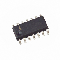
ISL6142IBZA Intersil, ISL6142IBZA Datasheet - Page 21

ISL6142IBZA
Manufacturer Part Number
ISL6142IBZA
Description
IC CTRLR HOT PLUG NEG 14-SOIC
Manufacturer
Intersil
Type
Hot-Swap Controllerr
Datasheet
1.ISL6142CBZA.pdf
(23 pages)
Specifications of ISL6142IBZA
Applications
General Purpose, VoIP
Internal Switch(s)
No
Voltage - Supply
36 V ~ 72 V
Operating Temperature
-40°C ~ 85°C
Mounting Type
Surface Mount
Package / Case
14-SOIC (0.154", 3.90mm Width)
Lead Free Status / RoHS Status
Lead free / RoHS Compliant
The switch SW1 is shown as a simple push button. It can be
replaced by an active switch, such as an NPN or NFET; the
principle is the same; pull the UV node below its trip point,
and then release it (toggle low). To connect an NFET, for
example, the DRAIN goes to UV; the source to -V
GATE is the input; if it goes high (relative to -V
NFET on, and UV is pulled low. Just make sure the NFET
resistance is low compared to the resistor divider, so that it
has no problem pulling down against it.
Applications: Layout Considerations
For the minimum application, there are 10 resistors, 3
capacitors, one IC and 2 FETs. A sample layout is shown in
Figure 39. It assumes the IC is 8-SOIC; Q1 is in a D2PAK (or
similar SMD-220 package).
Although GND planes are common with multi-level PCBs, for
a -48V system, the -48V rails (both input and output) act
more like a GND than the top 0V rail (mainly because the IC
signals are mostly referenced to the lower rail). So if
separate planes for each voltage are not an option, consider
prioritizing the bottom rails first.
Note that with the placement shown, most of the signal lines
are short, and there should be minimal interaction between
them.
Although decoupling capacitors across the IC supply pins
are often recommended in general, this application may not
need one, nor even tolerate one. For one thing, a decoupling
cap would add to (or be swamped out by) any other input
capacitance; it also needs to be charged up when power is
applied. But more importantly, there are no high speed (or
any) input signals to the IC that need to be conditioned. If still
-48V IN
GND
(SHORT PIN)
GND
D1*
Logic
Input
R10
Q2
21
(V
SW1*
Logic
Supply
EE
FIGURE 38. ISL6142/52 OPTIONAL COMPONENTS (SHOWN WITH *)
+5V)
C4*
ADC
TO
IN
R9
R4
R5
R6
), it turns the
IN
, and the
ISL6142, ISL6152
FAULT
DIS
IS
UV
OV
CT
C3
OUT
V
EE
IS-
R7
R1
R12 is a pull-up resistor for PWRGD, if there is no other
component acting as a pull-up device. The value of R12 is
determined by how much current is needed when the pin is
pulled low (also affected by the V
be pulled low enough for a good logic low level. An LED can
also be placed in series with R12, if desired. In that case, the
criteria is the LED brightness versus current.
desired, consider the isolation resistor R10, as shown in
figure 38.
NOTE:
R8
1. Layout scale is approximate; routing lines are just for illustration
2. Approximate size of the above layout is 0.8 x 0.8 inches,
3. R1 sense resistor is size 2512; all other R’s and C’s shown are
4. The RL and CL are not shown on the layout.
5. Vias are needed to connect R4 and V
6. PWRGD signal is not used here.
IS+
purposes; they do not necessarily conform to normal PCB
design rules. High current buses are wider, shown with parallel
lines.
excluding Q1 (D2PAK or similar SMD-220 package).
0805; they can all potentially use smaller footprints, if desired.
of the board, and R8 to pin 9; all other routing can be on the top
level.
ISL6142
SENSE GATE
V
DD
R11*
C1
Q1
R2
R3 C2
PWRGD
DRAIN
GND
DD
voltage); and it should
R12*
DD
-48V OUT
to GND on the bottom
RL
CL


