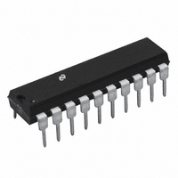
LMD18400N/NOPB National Semiconductor, LMD18400N/NOPB Datasheet

LMD18400N/NOPB
Specifications of LMD18400N/NOPB
*LMD18400N/NOPB
LMD18400N
Available stocks
Related parts for LMD18400N/NOPB
LMD18400N/NOPB Summary of contents
Page 1
... The LMD18400 is packaged in a special power dissipating leadframe that reduces the junction to case thermal resis- tance to approximately 20˚C/W. Typical Application © 2004 National Semiconductor Corporation Features n Four independent outputs with current capability n 1.3Ω maximum ON resistance over temperature ...
Page 2
Connection Diagram www.national.com 01102602 Order Number LMD18400N See NS Package Number N20A 2 ...
Page 3
... Absolute Maximum Ratings If Military/Aerospace specified devices are required, please contact the National Semiconductor Sales Office/ Distributors for availability and specifications. Supply Survival Voltage (Pin 20) Transient ( ms) Continuous Output Transient Current (Each Switch) Output Transient Current (Total, All Switches) Output Steady State Current ...
Page 4
Electrical Characteristics the entire operating temperature range, −25˚C ≤ T Parameter DIGITAL CHARACTERISTICS Logic “1” Input Voltage Logic “0” Input Voltage Logic “1” Input Current Logic “0” Input Current TRI-STATE Output Current Enable Input Current Channel Input Resistance Error Output ...
Page 5
Timing Specification Definitions Error Reporting Delay Typical Performance Characteristics perature unless otherwise noted. Switch ON Resistance vs Temperature Maximum Power Dissipation vs Ambient Temperature (Continued) 01102605 For all curves “Sleep Mode” Supply Current 01102631 01102633 5 Data Setup ...
Page 6
Typical Performance Characteristics temperature unless otherwise noted. (Continued) Clamp Characteristics vs Temperature Turn ON Rise Time vs Temperature Turn OFF Time vs Temperature www.national.com For all curves 12V, Temperature is the junction CC Error Sense Threshold Voltage vs ...
Page 7
Typical Performance Characteristics temperature unless otherwise noted. (Continued) Enable Threshold Voltage vs Temperature Functional Block Diagram For all curves 12V, Temperature is the junction CC 01102641 7 Error Output Voltage vs Sink Current 01102642 01102608 www.national.com ...
Page 8
Truth Table Enable Chip Select Switch Control Input Input Input (Pin 3) (Pin 4) (Pins 9, 10, 11, 12 Applications Information ...
Page 9
Applications Information 1.3Ω (the ON resistance of the DMOS switch). The voltage applied to the load will depend upon the load current and the designed current capability of the LMD18400. When a switch is commanded OFF, the load will be ...
Page 10
Applications Information FIGURE 4. Turn-OFF Conditions with an Inductive Load When the output inductance produces a negative voltage, the gate of the DMOS transistor is clamped at 0V. At −3.5V, the source of the power device is less than the ...
Page 11
Applications Information Thermal Protection The die temperature of the LMD18400 is continually moni- tored. Should any conditions cause the die temperature to rise to +170˚C, all of the power switches are turned OFF automatically to reduce the power dissipation. It ...
Page 12
Applications Information The Error Flag output pin is an open drain transistor which requires a pull-up resistor to a positive voltage 16V. Typically this pull- the same 5V supply which is biasing the Enable input ...
Page 13
Applications Information across it. Under this condition, an internal 50 kΩ resistor connected to V will provide a small amount of current to CC the load. If the load resistance is large enough to create a voltage greater than 4.1V ...
Page 14
Applications Information FIGURE 12. Recommended PC Board Layout to Reduce the Thermal Resistance from Junction-to-Ambient FIGURE 13. Switching an Inductive Load When switched ON, the worst case power dissipation is: The steady-state ON current of the inductor should be kept ...
Page 15
Applications Information FIGURE 14. Approximate time required for the die to reach the 170˚C thermal shutdown point from 25˚C for different ON/OFF Switching of Multiple Voltage Regulated Circuit Loads (Continued) 01102624 total package power dissipation levels. 15 01102625 www.national.com ...
Page 16
Applications Information Recommended Connection If No Diagnostics are Required www.national.com (Continued) Unipolar Drive for a 4-Phase Stepper Motor 16 01102626 01102627 ...
Page 17
Applications Information Simple protection of the LMD18400 against supply voltage reversal. Loads will be energized through the intrinsic diodes in parallel with the power switches. The Schottky diode will add approximately 0.2V to the logic input switching thresholds and the ...
Page 18
Applications Information Paralleling switches for higher current capability. Positive temperature coefficient of the switch ON resistance provides ballasting to evenly share the load current between the switches. Any combination of switches can be paralleled. Required peak load current will depend ...
Page 19
... BANNED SUBSTANCE COMPLIANCE National Semiconductor certifies that the products and packing materials meet the provisions of the Customer Products Stewardship Specification (CSP-9-111C2) and the Banned Substances and Materials of Interest Specification (CSP-9-111S2) and contain no ‘‘Banned Substances’’ as defined in CSP-9-111S2. ...


