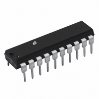
LMD18400N/NOPB National Semiconductor, LMD18400N/NOPB Datasheet - Page 13

LMD18400N/NOPB
Manufacturer Part Number
LMD18400N/NOPB
Description
IC DRIVER QUAD HI SIDE 20-DIP
Manufacturer
National Semiconductor
Datasheet
1.LMD18400NNOPB.pdf
(19 pages)
Specifications of LMD18400N/NOPB
Configuration
High-Side
Input Type
Non-Inverting
Delay Time
5µs
Current - Peak
3A
Number Of Configurations
4
Number Of Outputs
4
Voltage - Supply
7 V ~ 28 V
Operating Temperature
-25°C ~ 85°C
Mounting Type
Through Hole
Package / Case
20-DIP (0.300", 7.62mm)
Supply Voltage Min
7V
Supply Voltage Max
60V
No. Of Outputs
4
Output Voltage
5.5V
Output Current
3.75A
Driver Case Style
DIP
Msl
MSL 1 - Unlimited
Device Type
High Side
Rohs Compliant
Yes
Lead Free Status / RoHS Status
Lead free / RoHS Compliant
High Side Voltage - Max (bootstrap)
-
Other names
*LMD18400N
*LMD18400N/NOPB
LMD18400N
*LMD18400N/NOPB
LMD18400N
Available stocks
Company
Part Number
Manufacturer
Quantity
Price
Company:
Part Number:
LMD18400N/NOPB
Manufacturer:
National Semiconductor
Quantity:
135
Applications Information
across it. Under this condition, an internal 50 kΩ resistor
connected to V
the load. If the load resistance is large enough to create a
voltage greater than 4.1V an Open Load Error will be indi-
cated for that switch. The maximum load resistance that will
not generate an Open Load Error when a switch is OFF can
be found by:
To make this Open Load Error threshold more sensible, an
external pull-up resistor can be added from the output to the
V
Also when a switch is commanded OFF, should the load be
shorted to the V
indicate an error.
When a switch is commanded ON, the load is expected to
have a voltage across it that approaches the V
the output voltage is less than the 4.1V threshold an error will
again be reported, indicating that the load is either shorted to
ground or that the driver is in power limit and not able to pull
the output voltage any closer to V
resistance that will not generate a Shorted Load Error when
a switch is ON can be found by:
Figure 11 indicates the range of load resistance for normal
operation, open load, and shorted load or power limit indica-
tion.
CC
FIGURE 11. Load Resistance Detected as Errors
supply.
CC
CC
will provide a small amount of current to
supply, this same circuitry will again
CC
. The minimum load
(Continued)
CC
potential. If
01102620
13
THERMAL MANAGEMENT
It is particularly important to consider the total amount of
power being dissipated by all four switches in the LMD18400
at all times. Any combination of the switches driving loads
will cause an increase in the die temperature. Should the die
temperature reach the thermal shutdown threshold of
+170˚C, all of the switches will be disabled.
Careful calculation of the worst case total power dissipation
required at any point in time, together with providing suffi-
cient heatsinking will prevent this from occurring.
The LMD18400 is packaged with a special leadframe that
helps dissipate heat through the two ground pins on each
side of the package. The thermal resistance from junction-
to-case (θ
thermal resistance from junction-to-ambient (θ
any heatsinking, is approximately 60˚C/W. Figure 12 illus-
trates how the copper foil of a printed circuit board can be
designed to provide heatsinking and reduce the overall
junction-to-ambient thermal resistance.
The power dissipation in each switch is equal to:
where R
mum). These equations hold true until the power dissipation
reaches the maximum limit of 15W. With resistive loads, the
15W power limit threshold will be reached when:
Inductive loads will create additional power dissipation when
switched OFF. Figure 13 shows the idealized voltage and
current waveforms for an inductive load.
ON
JC
) for this package is approximately 20˚C/W. The
is the ON resistance of the switch (1.3Ω maxi-
JA
www.national.com
), without


