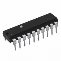
LMD18400N/NOPB National Semiconductor, LMD18400N/NOPB Datasheet - Page 12

LMD18400N/NOPB
Manufacturer Part Number
LMD18400N/NOPB
Description
IC DRIVER QUAD HI SIDE 20-DIP
Manufacturer
National Semiconductor
Datasheet
1.LMD18400NNOPB.pdf
(19 pages)
Specifications of LMD18400N/NOPB
Configuration
High-Side
Input Type
Non-Inverting
Delay Time
5µs
Current - Peak
3A
Number Of Configurations
4
Number Of Outputs
4
Voltage - Supply
7 V ~ 28 V
Operating Temperature
-25°C ~ 85°C
Mounting Type
Through Hole
Package / Case
20-DIP (0.300", 7.62mm)
Supply Voltage Min
7V
Supply Voltage Max
60V
No. Of Outputs
4
Output Voltage
5.5V
Output Current
3.75A
Driver Case Style
DIP
Msl
MSL 1 - Unlimited
Device Type
High Side
Rohs Compliant
Yes
Lead Free Status / RoHS Status
Lead free / RoHS Compliant
High Side Voltage - Max (bootstrap)
-
Other names
*LMD18400N
*LMD18400N/NOPB
LMD18400N
*LMD18400N/NOPB
LMD18400N
Available stocks
Company
Part Number
Manufacturer
Quantity
Price
Company:
Part Number:
LMD18400N/NOPB
Manufacturer:
National Semiconductor
Quantity:
135
www.national.com
Applications Information
The Error Flag output pin is an open drain transistor which
requires a pull-up resistor to a positive voltage of up to 16V.
Typically this pull-up is to the same 5V supply which is
biasing the Enable input and any other external logic cir-
cuitry. The Error Flag pins of several LMD18400 packages
can be connected together with just one pull-up resistor to
provide an all-encompassing general system error indica-
tion. Upon detection of an error, each device could then be
polled for diagnostic information to determine the source of
the fault condition.
A second direct output error flag is for an indication of
Thermal Shutdown (pin 17). This active low flag provides an
immediate indication that the die temperature has reached
+170˚C and that the drive to all four switches has been
removed. This output is pulled up to the internal 5.1V logic
regulator through a small (5 µA) current source so use of a
buffer on this pin is recommended.
A useful feature of pin 17 is that it can also be used as a
shutdown input. Driving this pin low immediately switches all
of the drivers OFF, just the same as if thermal shutdown
temperatures has been reached, yet all of the control logic
and diagnostic circuits remain active. This is useful in de-
signing “fail-safe” systems where the loads can be disabled
FIGURE 9. Thermal Shutdown Flag and Shutdown
Input
FIGURE 8. Serial Diagnostic Data Assignments
(Continued)
01102618
12
under any sort of externally detected system fault condition.
The diagnostic logic however does not distinguish between
normal thermal shutdown or the fact that pin 17 has been
driven low. As such, various switch errors and an over-
temperature indication will be reported in the diagnostic data
stream.
Figure 9 illustrates the use of pin 17 as both an output
thermal shutdown flag and as an input to shut down only the
switches. Directly tying pin 17 to +5V will prevent the internal
thermal shutdown circuitry from disabling the switches. For
reliability purposes however this is not recommended as
there will then be no limit to the maximum die temperature.
Refer to the Truth Table for a summary of the action of these
direct-output error flags.
LOAD ERROR DETECTION
An important feature of the LMD18400 is the ability to detect
open or shorted load connections. Figure 10 illustrates the
detection circuit used with each of the drivers.
A voltage comparator monitors the voltage to the load and
compares it to a fixed 4.1V reference level. When a switch is
OFF, the ground referenced load should have no voltage
FIGURE 10. Detection Circuitry for Open/Shorted
Loads
01102609
01102617


