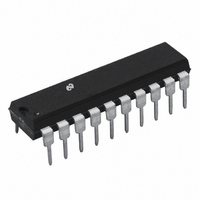
LMD18400N/NOPB National Semiconductor, LMD18400N/NOPB Datasheet - Page 4

LMD18400N/NOPB
Manufacturer Part Number
LMD18400N/NOPB
Description
IC DRIVER QUAD HI SIDE 20-DIP
Manufacturer
National Semiconductor
Datasheet
1.LMD18400NNOPB.pdf
(19 pages)
Specifications of LMD18400N/NOPB
Configuration
High-Side
Input Type
Non-Inverting
Delay Time
5µs
Current - Peak
3A
Number Of Configurations
4
Number Of Outputs
4
Voltage - Supply
7 V ~ 28 V
Operating Temperature
-25°C ~ 85°C
Mounting Type
Through Hole
Package / Case
20-DIP (0.300", 7.62mm)
Supply Voltage Min
7V
Supply Voltage Max
60V
No. Of Outputs
4
Output Voltage
5.5V
Output Current
3.75A
Driver Case Style
DIP
Msl
MSL 1 - Unlimited
Device Type
High Side
Rohs Compliant
Yes
Lead Free Status / RoHS Status
Lead free / RoHS Compliant
High Side Voltage - Max (bootstrap)
-
Other names
*LMD18400N
*LMD18400N/NOPB
LMD18400N
*LMD18400N/NOPB
LMD18400N
Available stocks
Company
Part Number
Manufacturer
Quantity
Price
Company:
Part Number:
LMD18400N/NOPB
Manufacturer:
National Semiconductor
Quantity:
135
www.national.com
DIGITAL CHARACTERISTICS
Logic “1” Input Voltage
Logic “0” Input Voltage
Logic “1” Input Current
Logic “0” Input Current
TRI-STATE Output Current
Enable Input Current
Channel Input Resistance
Error Output Sink Current
Logic “1” Output Voltage
Logic “0” Output Voltage
Thermal Shutdown Output Source
Current
Thermal Shutdown Output Sink Current
Electrical Characteristics
the entire operating temperature range, −25˚C ≤ T
Note 1: Absolute Maximum Ratings indicate limits beyond which damage to the device may occur. Operating Ratings indicate conditions for which the device is
intended to be functional, but do not guarantee specific performance limits. For guaranteed specifications and test conditions, see the Electrical Characteristics.
Note 2: Human body model; 100 pF discharge through a 1.5 kΩ resistor. All pins except pins 8 and 13 which are protected to 1000V and pins 1, 2, 18 and 19 which
are protected to 500V.
Note 3: The maximum power dissipation is a function of T
ambient temperature is P
shutdown. For the LMD18400 the junction-to-ambient thermal resistance, θ
the package will be, I
Note 4: Typical values are at T
Note 5: All limits are 100% production tested at +25˚C. Limits at temperature extremes are guaranteed through correlation and accepted Statistical Quality Control
(SQC) methods.
Note 6: Pulse Testing techniques used. Pulse width is
Timing Specification Definitions
Parameter
DC MAX
Switching Turn ON/OFF
D
= (T
2
x R
J MAX
J
ON (MAX)
= +25˚C and represent the most likely parametric norm.
–T
A
)/θ
x 4 switches 1A
JA
. If this dissipation is exceeded, the die temperature will rise above 150˚C and the device will eventually go into thermal
V
Pins 3, 4, 7, 9, 10, 11, 12
Pins 3, 4, 7, 9, 10, 11, 12
Pins 4, 7
Pins 4, 7
Pin 8, Pin 4 = 5V
Pin 8 = 0V
Pin 3 = 2.4V
Pins 9, 10, 11, 12
Pin 13 = 0.8V
Pin 8
I
I
I
Pin 8
I
Pin 17 = 2.4V
Pin 17 = 0.8V
OUT
OUT
OUT
OUT
<
CC
2
5 ms with a duty cycle
J MAX
x 1.3Ω x 4 = 5.2W).
= 12V, C
= −360 µA
= −10 µA
= −10 µA
= 100 µA
, θ
A
JA
≤ +85˚C, all other limits are for T
, and T
01102603
CP
Conditions
JA
A
= 0.01 µFd, unless otherwise indicated. Boldface limits apply over
and is limited by thermal shutdown. The maximum allowable power dissipation at any
, is 60˚C/W. With sufficient heatsinking the maximum continuous power dissipation for
4
<
1%.
A
= T
Enable Turn-On
(Note 4)
Typical
−0.001
J
0.001
−0.05
0.05
360
4.4
5.1
12
75
= +25˚C. (Continued)
4
5
(Note 5)
Limit
−10
250
2.0
0.8
1.6
2.4
4.5
5.5
0.4
−1
10
25
15
1
3
01102604
µA (Max)
µA (Max)
µA (Max)
µA (Max)
µA (Max)
mA (Min)
kΩ (Min)
µA (Min)
µA (Min)
V (Max)
V (Max)
V (Min)
V (Min)
V (Min)
V (Min)
(Limit)
Units


