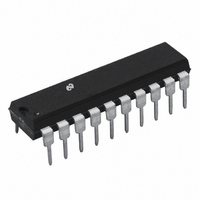
LMD18400N/NOPB National Semiconductor, LMD18400N/NOPB Datasheet - Page 3

LMD18400N/NOPB
Manufacturer Part Number
LMD18400N/NOPB
Description
IC DRIVER QUAD HI SIDE 20-DIP
Manufacturer
National Semiconductor
Datasheet
1.LMD18400NNOPB.pdf
(19 pages)
Specifications of LMD18400N/NOPB
Configuration
High-Side
Input Type
Non-Inverting
Delay Time
5µs
Current - Peak
3A
Number Of Configurations
4
Number Of Outputs
4
Voltage - Supply
7 V ~ 28 V
Operating Temperature
-25°C ~ 85°C
Mounting Type
Through Hole
Package / Case
20-DIP (0.300", 7.62mm)
Supply Voltage Min
7V
Supply Voltage Max
60V
No. Of Outputs
4
Output Voltage
5.5V
Output Current
3.75A
Driver Case Style
DIP
Msl
MSL 1 - Unlimited
Device Type
High Side
Rohs Compliant
Yes
Lead Free Status / RoHS Status
Lead free / RoHS Compliant
High Side Voltage - Max (bootstrap)
-
Other names
*LMD18400N
*LMD18400N/NOPB
LMD18400N
*LMD18400N/NOPB
LMD18400N
Available stocks
Company
Part Number
Manufacturer
Quantity
Price
Company:
Part Number:
LMD18400N/NOPB
Manufacturer:
National Semiconductor
Quantity:
135
DC CHARACTERISTICS
Supply Current
Output Leakage
Rds ON
Short Circuit Current
Maximum Output Current
Lead Error Threshold Voltage
Open Load Detection Current
Negative Clamp Output Voltage
Overvoltage Shutdown Threshold
Overvoltage Shutdown Hysteresis
Error Output Leakage Current
Thermal Warning Temperature
Thermal Shutdown Temperature
Thermal Warning Temperature
AC CHARACTERISTICS
Switch Turn-On Delay (t
Switch Turn-On Rise Time (t
Switch Turn-Off Delay (t
Switch Turn-Off Fall Time (t
Enable Time (t
Error Reporting Delay (t
Data Setup Time (t
TRI-STATE
Data Clock Frequency
Absolute Maximum Ratings
If Military/Aerospace specified devices are required,
please contact the National Semiconductor Sales Office/
Distributors for availability and specifications.
Electrical Characteristics
over the entire operating temperature range, −25˚C ≤ T
Supply Survival Voltage (Pin 20)
Output Transient Current (Each Switch)
Output Transient Current
Output Steady State Current
Logic Input Voltage
Transient (t = 10 ms)
Continuous
(Total, All Switches)
(Each Switch)
(Pins 3, 9, 10, 11, 12)
®
Control (t
EN
Parameter
)
DS
)
1H
Error
d(ON)
d(OFF)
, t
OH
OFF
)
ON
)
)
)
)
)
Enable Input = 0V
Enable Input = 5V, Inputs = 0V
Enable Input = 5V, Inputs = 5V
Open Loads
Enable Input = 0V, Inputs = 0V
(Pins 1, 2, 18, 19)
I
V
V
V
V
Pins 1, 2, 18, 19
Pins 1, 2, 18, 19
I
V
V
V
V
Enable (Pin 3) = 5V, I
I
Enable (Pin 3) = 5V, I
I
Measured with Switch 1, Pin 9 = 5V
Enable (Pin 3) = 5V, Switch 1 Load
Opened
C
Pin 8, Hi-Z Enable Time
OUT
O
OUT
OUT
V
−0.5V to +60V
−0.3V to +16V
CC
CC
CC
CC
PIN 13
PIN 13
PIN 17
PIN 13
L
CC
= 1A, (Note 6)
= 30 pF
(Note 1)
= 12V, (Note 6)
= 7V, (Note 6)
= 28V, (Note 6)
−V
= 1A, (Note 6)
= 1A
= 1A
= 12V, C
O
= 12V
<
<
<
= 4V, (Note 6)
0.8V
0.8V
0.8V
3.75A
80V
A
6A
1A
≤ +85˚C, all other limits are for T
Conditions
CP
= 0.01 µFd, unless otherwise indicated. Boldface limits apply
3
OUT
OUT
Operating Ratings
Logic Input Voltage (Pins 4, 7)
Error Flag Voltage
ESD Susceptibility (Note 2)
Power Dissipation (Note 3)
Junction Temperature (T
Storage Temperature Range
Lead Temperature (Soldering, 10 sec.)
Ambient Temperature Range (T
Supply Voltage Range
= 1A
= 1A
(Note 4)
Typical
0.001
A
0.04
0.01
3.75
0.75
0.15
150
145
170
145
200
7.5
7.5
0.8
1.2
2.4
0.6
4.1
0.5
−5
31
30
75
J MAX
= T
5
7
2
3
J
150˚C)
= +25˚C.
(Note 1)
A
)
(Note 5)
Limit
300
150
500
1.3
0.6
10
15
15
40
10
10
15
50
2
1
1
Internally Limited
−65˚C to +150˚C
−25˚C to +85˚C
−0.3V to +6V
www.national.com
7V to 28V
MHz (Max)
mA (Max)
mA (Max)
µA (Max)
µA (Max)
µA (Max)
µs (Max)
µs (Max)
µs (Max)
µs (Max)
µs (Max)
µs (Max)
Ω (Max)
ns (Min)
V (Max)
+260˚C
A (Min)
(Limit)
2000V
Units
150˚C
µA
˚C
˚C
˚C
µs
A
A
A
V
V
V
16V
5W


