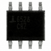
ISL6528CBZ-T Intersil, ISL6528CBZ-T Datasheet - Page 10

ISL6528CBZ-T
Manufacturer Part Number
ISL6528CBZ-T
Description
IC CTRLR PWM BUCK DUAL 8-SOIC
Manufacturer
Intersil
Datasheet
1.ISL6528CBZ-T.pdf
(13 pages)
Specifications of ISL6528CBZ-T
Pwm Type
Voltage Mode
Number Of Outputs
2
Frequency - Max
650kHz
Duty Cycle
100%
Voltage - Supply
4.5 V ~ 5.5 V
Buck
Yes
Boost
No
Flyback
No
Inverting
No
Doubler
No
Divider
No
Cuk
No
Isolated
No
Operating Temperature
0°C ~ 70°C
Package / Case
8-SOIC (3.9mm Width)
Frequency-max
650kHz
Peak Reflow Compatible (260 C)
Yes
Rohs Compliant
Yes
Lead Free Status / RoHS Status
Lead free / RoHS Compliant
Other names
ISL6528CBZ-TTR
inductance value will slow the converter response time to a
load transient.
One of the parameters limiting the converter’s response to a
load transient is the time required to slew the inductor
current. Given a sufficiently fast control loop design, the
ISL6528 will provide either 0% or 100% duty cycle in
response to a load transient. The response time is the time
interval required to slew the inductor current from an initial
current value to the final current level. During this interval the
difference between the inductor current and the load current
must be supplied by the output capacitor(s). Minimizing the
response time can minimize the output capacitance
required.
The response time to a transient is different for the
application of load and the removal of load. The following
equations give the approximate response time interval for
application and removal of a transient load:
where I
response time to the application of load, and t
response time to the removal of load.
With a +3.3V input source, the worst case response time can
be either at the application or removal of load and dependent
upon the output voltage setting. Be sure to check both of
these equations at the minimum and maximum output levels
for the worst case response time.
Input Capacitor Selection
The important parameters for the bulk input capacitors are
the voltage rating and the RMS current rating. For reliable
operation, select bulk input capacitors with voltage and
current ratings above the maximum input voltage and largest
RMS current required by the circuit. The capacitor voltage
rating should be at least 1.25 times greater than the
maximum input voltage and a voltage rating of 1.5 times is a
conservative guideline. The RMS current rating requirement
for the input capacitor of a buck regulator is approximately
1/2 of the summation of the DC load current.
Use a mix of input bypass capacitors to control the voltage
overshoot across the MOSFETs. Use ceramic capacitance
for the high frequency decoupling and bulk capacitors to
supply the RMS current. Small ceramic capacitors can be
placed very close to the upper MOSFET to suppress the
voltage induced in the parasitic circuit impedances. Connect
them directly to ground with a via placed very close to the
ceramic capacitor footprint.
t
t
RISE
FALL
=
=
TRAN
------------------------------- -
V
L
L
------------------------------ -
O
O
IN
V
×
×
–
OUT
I
I
is the transient load current step, t
V
TRAN
TRAN
OUT
10
FALL
RISE
is the
(EQ. 13)
(EQ. 14)
is the
ISL6528
For a through-hole design, several aluminum electrolytic
capacitors may be needed. For surface mount designs,
tantalum or special polymer capacitors can be used, but
caution must be exercised with regard to the capacitor surge
current rating. These capacitors must be capable of handling
the surge-current at power-up.
Transistor Selection/Considerations
The ISL6528 requires two external transistors. One N-
channel MOSFET is used as the upper switch in a standard
buck topology PWM converter. The linear controller drives
an NPN bipolar transistor as a pass element. The transistors
should be selected based upon r
saturation voltages, gate/base supply requirements, and
thermal management considerations.
UPPER MOSFET SWITCH SELECTION
In high-current applications, the MOSFET power dissipation,
package selection and heatsink are the dominant design
factors. The power dissipation includes two loss
components; conduction loss and switching loss. The
conduction losses account for a large portion of the power
dissipation of the MOSFET. Switching losses also contribute
to the overall MOSFET power loss.
where I
the converter (defined as V
interval, and F
These equations assume linear voltage-current transitions
and are approximations. The gate-charge losses are
dissipated by the ISL6528 and do not heat the MOSFET.
However, large gate-charge increases the switching interval,
t
Ensure that the MOSFET is within its maximum junction
temperature at high ambient temperature by calculating the
temperature rise according to package thermal-resistance
specifications. A separate heatsink may be necessary
depending upon MOSFET power, package type, ambient
temperature, air flow, and load current requirements.
Given the reduced available gate bias voltage (5V) a logic-
level transistor is recommended for the upper switch. Close
attention to layout guidelines should be exercised with
devices exhibiting very low V
low gate threshold could lead to some shoot-through despite
counteracting circuitry present aboard the ISL6528.
NPN PASS TRANSISTOR SELECTION
A bipolar NPN transistor must be used with the linear
controller. Insure the current gain at the given operating V
is sufficiently large to provide the desired maximum output
P
P
SW
Conduction
Switching
, which increases the upper MOSFET switching losses.
o
is the maximum load current, D is the duty cycle of
≅
≅
1
-- - I
2
I
SW
o
2
o
×
×
V
r
is the PWM switching frequency.
DS on
IN
(
×
t
SW
)
×
D
×
O
F
/V
GS(on)
SW
IN
DS(ON)
), t
SW
characteristics, as the
is the switching
, current gain,
March 9, 2006
(EQ. 15)
(EQ. 16)
FN9038.4
CE


